

Core board comprising nickel layer, multilayer board and manufacturing method thereof
a nickel layer and core board technology, applied in the field of core boards, can solve the problems of weakening the binding strength of conductive layers, not being suitable for efficient semi-additive methods, and not being suitable for use as core materials, so as to achieve the effect of improving the binding strength
Inactive Publication Date: 2007-08-30
SAMSUNG ELECTRO MECHANICS CO LTD
View PDF54 Cites 2 Cited by
- Summary
- Abstract
- Description
- Claims
- Application Information
AI Technical Summary
Benefits of technology
The present invention provides a core board and a manufacturing method with improved binding strength between an insulation layer and a conductive layer, allowing for fine inner circuits to be formed. The manufacturing method includes a plating time that is 10% of conventional methods, resulting in reduced plating time and a thinner nickel layer. The method also includes selective etching during the flash etching process, reducing etching time and the occurrence of dangerous under cut. Additionally, the invention provides a multilayer board with reduced plating time and thickness of the nickel layer, reducing manufacturing costs. The use of sodium hypophosphate as a reducing agent in electroless copper plating results in improved binding strength and reduced environmental pollution. The invention also provides a method for manufacturing a core board with improved binding strength and reduced plating time. Overall, the invention improves the manufacturing process for core boards and multilayer boards.
Problems solved by technology
However, since binding strength between a copper foil layer and an insulation layer forming the CCL is weak due to thick thickness of the copper foil layer of CCL, it is not suitable to efficiently apply the semi-additive method.
In order to form fine circuits has costly Animoto build-up film(ABF) been used, and it is thus not suitable to use as core materials.
However, binding strength towards conductive layers gets weaker with more using of such additives.
However, there is still no solution to improve the binding strength of the conductive layer.
Method used
View moreImage
Smart ImageViewing Examples

Examples
example
[0059]
SodiumTempRoadNickelhypophosphateSuccinicTime(° C.)(dm2 / L)sulfate(g / L)(g / L)acid(g / L)pH(min)Plating75–900.1–14–4.820–505–304.2–4.82–4conditions
[0060]After a nickel plating layer having a thickness of 0.4-1 μm was formed on glass epoxy laminate(FR-4) by the above plating conditions three times, each peel strength was determined. The result is summarized in Table 1. A nickel plating layer having a thickness of 0.4-1 μm was also formed on BT-resin by the same plating conditions and its peel strength was determined. The result is summarized in Table 1. It is noted that the peel strength of the nickel plating layer is superior to that of the electroless copper plating layer.
Login to View More PUM
| Property | Measurement | Unit |
|---|---|---|
| thickness | aaaaa | aaaaa |
| wiring distance | aaaaa | aaaaa |
| temperature | aaaaa | aaaaa |
Abstract
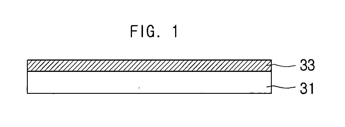
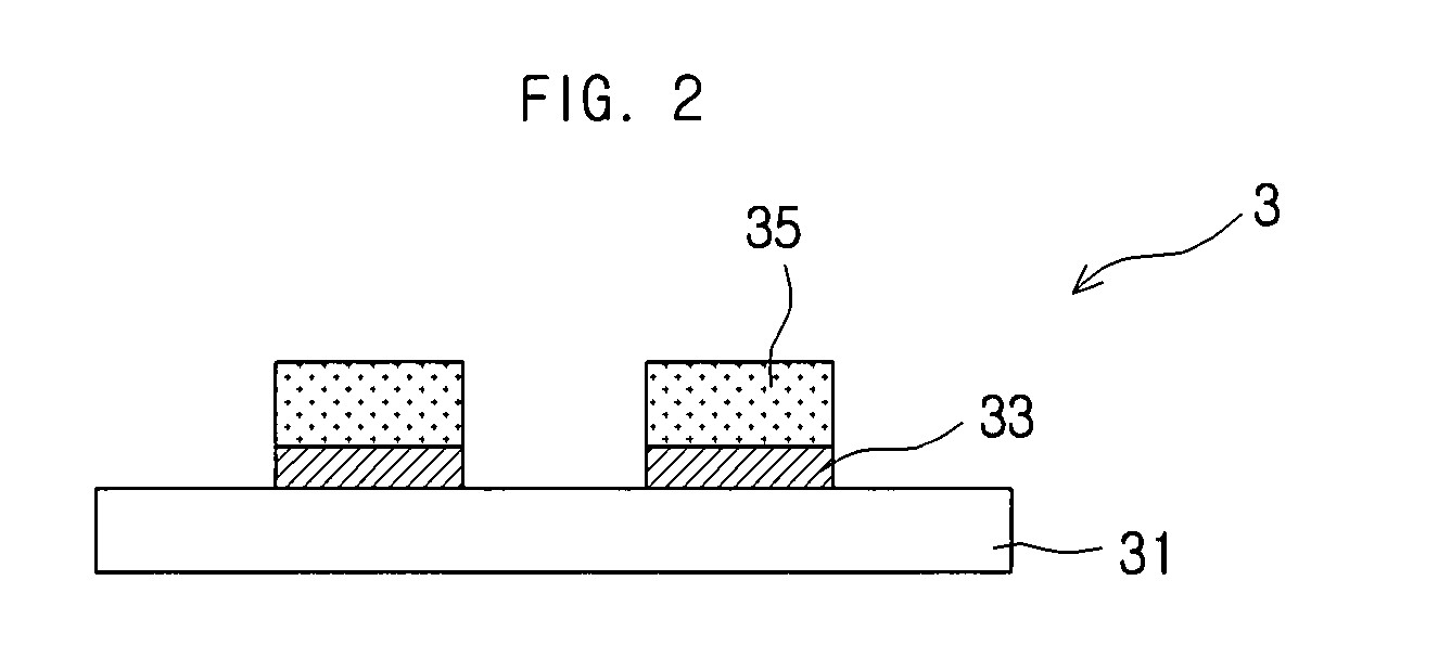
The present invention provides a core board and a manufacturing method thereof, in which the core board includes a nickel layer as a seed layer to improve the binding strength between an insulation layer and a conductive layer, so that it allows forming fine inner circuits by the semi-additive method.
Description
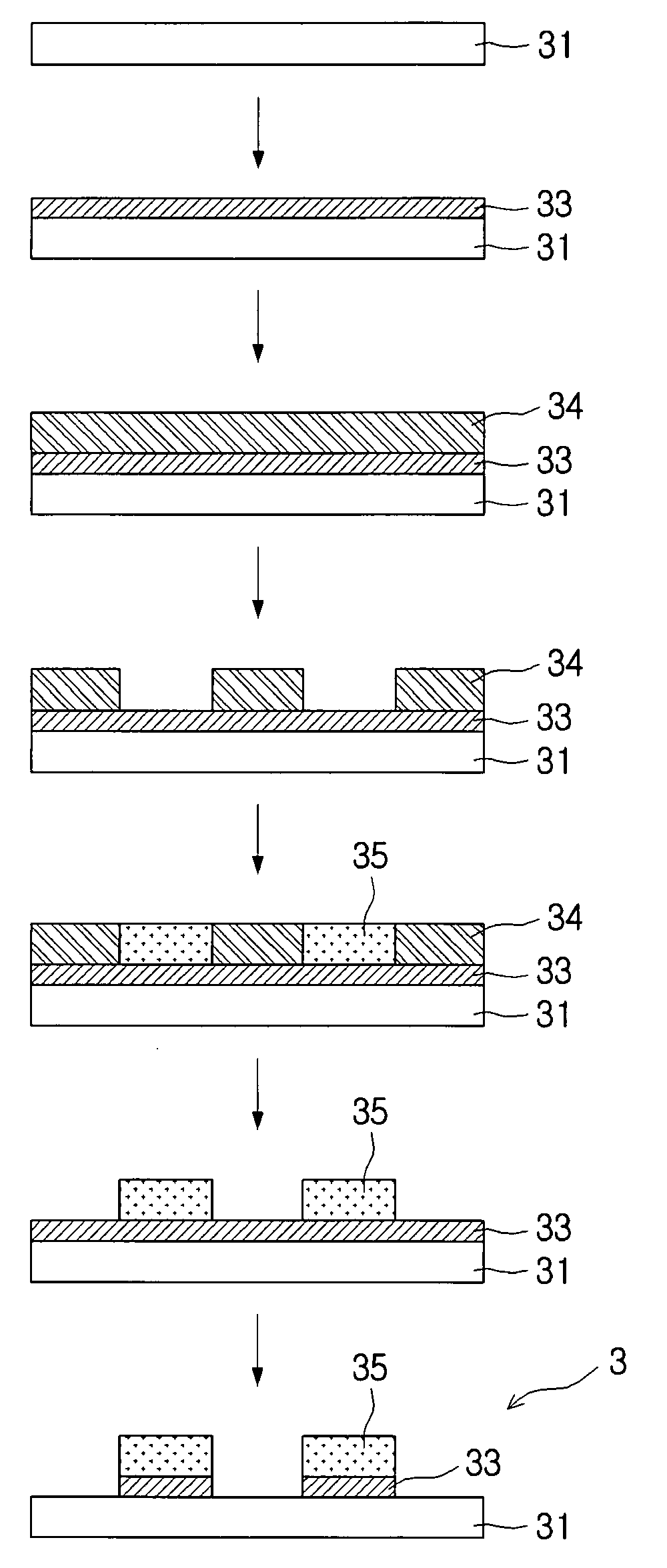
CROSS-REFERENCE TO RELATED APPLICATIONS[0001]This application claims the benefit of Korean Patent Application No. 2006-18241 filed with the Korea Industrial Property Office on Feb. 24, 2006, the disclosure of which is incorporated herein by reference in their entirety.BACKGROUND[0002]1. Technical Field[0003]The present invention relates to a board and a manufacturing method thereof, and more particularly, to a board having excellent joining strength between an insulation layer and a conductive layer, and a manufacturing method thereof.[0004]2. Description of the Related Art[0005]As electric components become much smaller, thinner, lighter, and more efficient, there is an increasing demand for component materials providing the corresponding performances. Boards as such a component material should satisfy high densification, thin plating, miniaturization, packaging, and the like and particularly, researches on a variety of kinds of boards used in highly integrated components have been...
Claims
Login to View More Application Information
Patent Timeline
 Patent Type & AuthorityApplications(United States)
IPC IPC(8): H05K7/00B32B15/04B05D5/12B28B19/00H05K3/00
CPCH05K3/108H05K3/181Y10T29/49124H05K2201/0344H05K3/4661Y10T428/31678A47C7/448A47C27/146A61H39/04
InventorJUNG, SOON-OHCHOI, CHEOL-HONAM, CHANG-HYUNKIM, HONG-WONKIM, SEUNG-CHUL
OwnerSAMSUNG ELECTRO MECHANICS CO LTD