Integrated CMOS and MEMS with air dielectric method and system

a technology of air dielectric and integrated cmos, which is applied in the field of integrated devices, can solve the problems of increasing the cost of mems development, focusing on mems development, and still having limitations, and achieves the effects of reducing metal line coupling, signal interference, and other related issues

Active Publication Date: 2013-04-16
MOVELLA INC
View PDF7 Cites 50 Cited by
  • Summary
  • Abstract
  • Description
  • Claims
  • Application Information

AI Technical Summary

Benefits of technology

[0009]Embodiments of the present invention can provide many benefits over conventional techniques. For example, the present technique provides an easy to use process that relies upon conventional technology. In some embodiments, the method provides higher device yields in dies per wafer with the integrated approach. Additionally, the method provides a process and system that are compatible with conventional process technology without substantial modifications to conventional equipment and processes. In a specific embodiment, the air dielectric regions can reduce metal line coupling, capacitance, signal interference, and other related issues. Also, these regions can reduce parasitic coupling to the substrate, reduce signal loss, and reduce power while increasing bandwidth. These benefits, as well as others, can be used to achieve higher performance (i.e. less reflection and lower power) in antennas and lower loss and higher isolation in transmission lines. Preferably, embodiments of the invention provide for an improved MEMS device system and related applications for a variety of uses. One or more embodiments of the present invention provide for all MEMS and related applications, which may be integrated on one or more CMOS device structures. Depending upon the embodiment, one or more of these benefits may be achieved. These and other benefits will be described in more throughout the present specification and more particularly below.

Problems solved by technology

Although highly successful, ICs and in particular MEMS still have limitations.
Similar to IC development, MEMS development, which focuses on increasing performance, reducing size, and decreasing cost, continues to be challenging.
Additionally, applications of MEMS often require increasingly complex microsystems that desire greater computational power.
Unfortunately, such applications generally do not exist.

Method used


Image

  • Integrated CMOS and MEMS with air dielectric method and system
  • Integrated CMOS and MEMS with air dielectric method and system
  • Integrated CMOS and MEMS with air dielectric method and system

Examples


Embodiment Construction

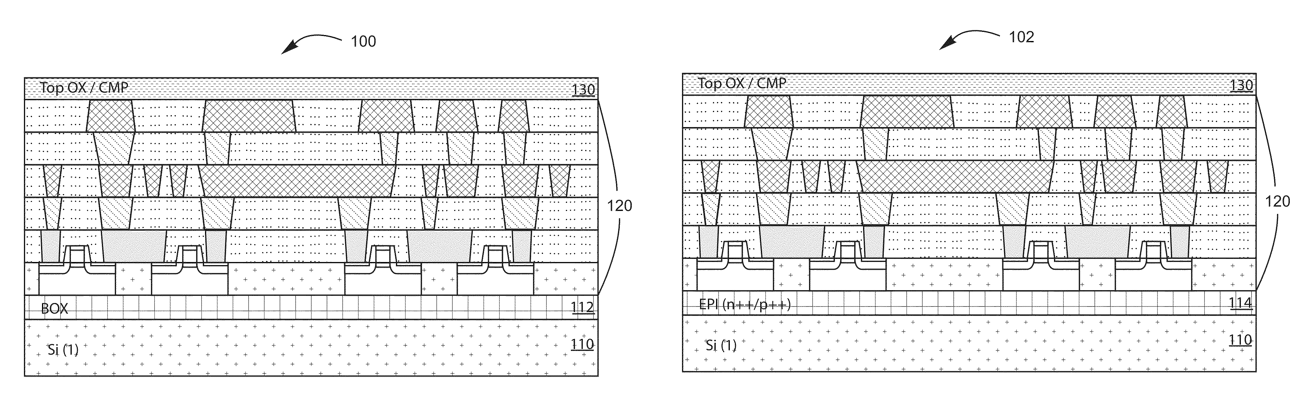
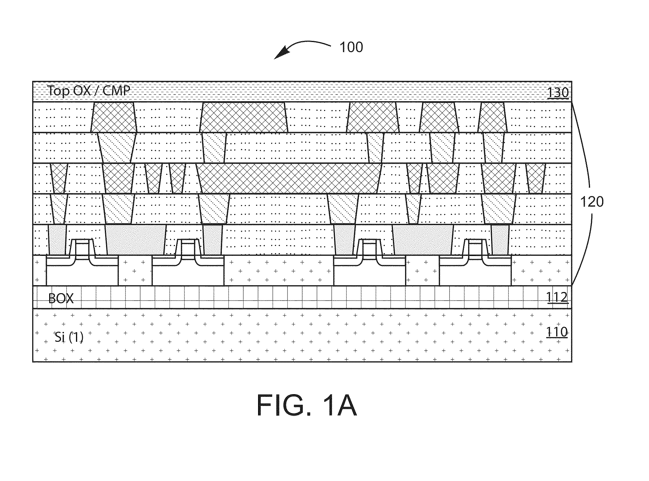
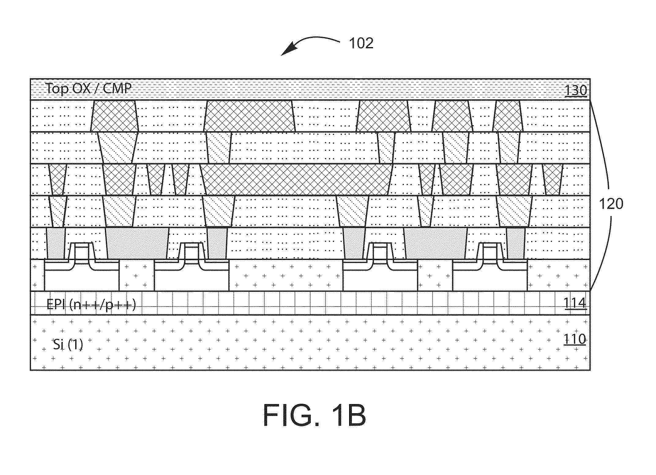
[0032]According to the present invention, techniques related generally to integrated devices and systems are provided. More particularly, the present invention provides a method for fabricating an integrated CMOS and MEMS device using an air dielectric. More specifically, the present invention provides a method for bonding semiconductor materials to form one or more air dielectric regions within an integrated CMOS and MEMS device. Merely by way of example, the MEMS devices can include at least an accelerometer, a gyroscope, a magnetic sensor, a pressure sensor, a microphone, a humidity sensor, a temperature sensor, a chemical sensor, a biosensor, an inertial sensor, and others. Additionally, the other applications include at least a sensor application or applications, system applications, and broadband applications, among others. But it will be recognized that the invention has a much broader range of applicability.

[0033]FIGS. 1A-1C are simplified cross-section diagrams of an integr...


PUM


Abstract

A method and structure for fabricating a monolithic integrated CMOS and MEMS device. The method includes providing a first semiconductor substrate having a first surface region and forming one or more CMOS IC devices on a CMOS IC device region overlying the first surface region. The CMOS IC device region can also have a CMOS surface region. A bonding material can be formed overlying the CMOS surface region to form an interface by which a second semiconductor substrate can be joined to the CMOS surface region. The second semiconductor substrate having a second surface region to the CMOS surface region by bonding the second surface region to the bonding material, the second semiconductor substrate comprising one or more first air dielectric regions. One or more free standing MEMS structures can be formed within one or more portions of the processed first substrate.

Description

CROSS-REFERENCES TO RELATED APPLICATIONS[0001]The present application claims priority to and incorporates by reference, for all purposes, the following patent application: U.S. Pat. App. No. 61 / 296,432, filed Jan. 19, 2010. The present invention also incorporates by reference, for all purposes, the following co-pending patent applications related to CMOS & MEMS devices and IC fabrication methodology: U.S. patent application Ser. No. 12 / 490,067, filed Jun. 23, 2009, U.S. patent application Ser. No. 12 / 717,070, filed Mar. 3, 2010, U.S. patent application Ser. No. 12 / 945,087, filed Nov. 12, 2010, and U.S. patent application Ser. No. 12 / 945,834, filed Nov. 13, 2010.BACKGROUND OF THE INVENTION[0002]Embodiments of the present invention relate generally to integrated devices. More particularly, embodiments of the present invention provide a method for fabricating an integrated CMOS and MEMS device using an air dielectric. More specifically, embodiments of the present invention provide a me...

Claims


Application Information

Patent Timeline
Patent Type & Authority Patents(United States)
IPC IPC(8): H01L27/108
CPCB81C1/00246H01L27/0688B81C2203/0771B81C2203/0735H01L27/0617H01L2224/48091B81C1/00238H01L27/092H01L29/0649H01L2924/00014B81B7/0038B81B7/008B81B2207/094H01L21/8221
Inventor YANG, XIAO "CHARLES"
Owner MOVELLA INC
Why Eureka
Try Eureka