Structure and method of fabricating a CZTS photovoltaic device by electrodeposition

a photovoltaic device and electrodeposition technology, applied in the direction of solid-state devices, semiconductor devices, basic electric elements, etc., can solve the problems of difficult to uniformly deposit material over large areas, costly vacuum deposition,

Inactive Publication Date: 2013-04-23
GLOBALFOUNDRIES INC
View PDF19 Cites 12 Cited by
  • Summary
  • Abstract
  • Description
  • Claims
  • Application Information

AI Technical Summary

Problems solved by technology

Vacuum deposition is however costly.
Further, with vacuum deposition it is difficult to deposit the material over large areas uniformly.

Method used


Image

  • Structure and method of fabricating a CZTS photovoltaic device by electrodeposition
  • Structure and method of fabricating a CZTS photovoltaic device by electrodeposition
  • Structure and method of fabricating a CZTS photovoltaic device by electrodeposition

Examples


Embodiment Construction

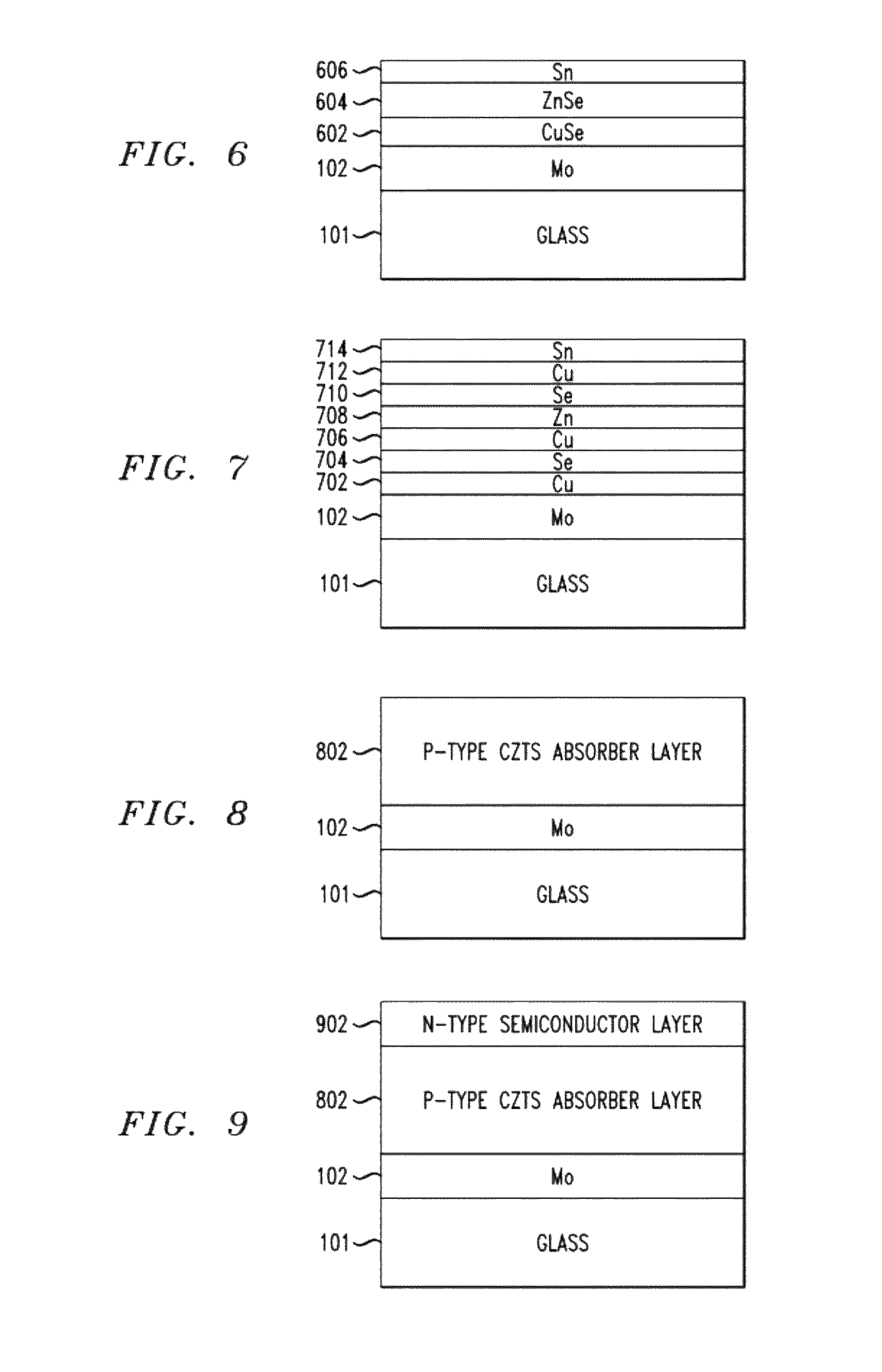
[0032]Provided herein is an electrodeposition process for the fabrication of Cu2ZnSn(S,Se)4 (CZTS) p-type absorber materials for solar cell applications. Electrodeposition is much cheaper than any vacuum process and allows the fabrication of large areas with excellent thickness uniformity and compositional uniformity.

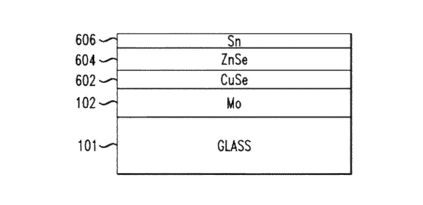
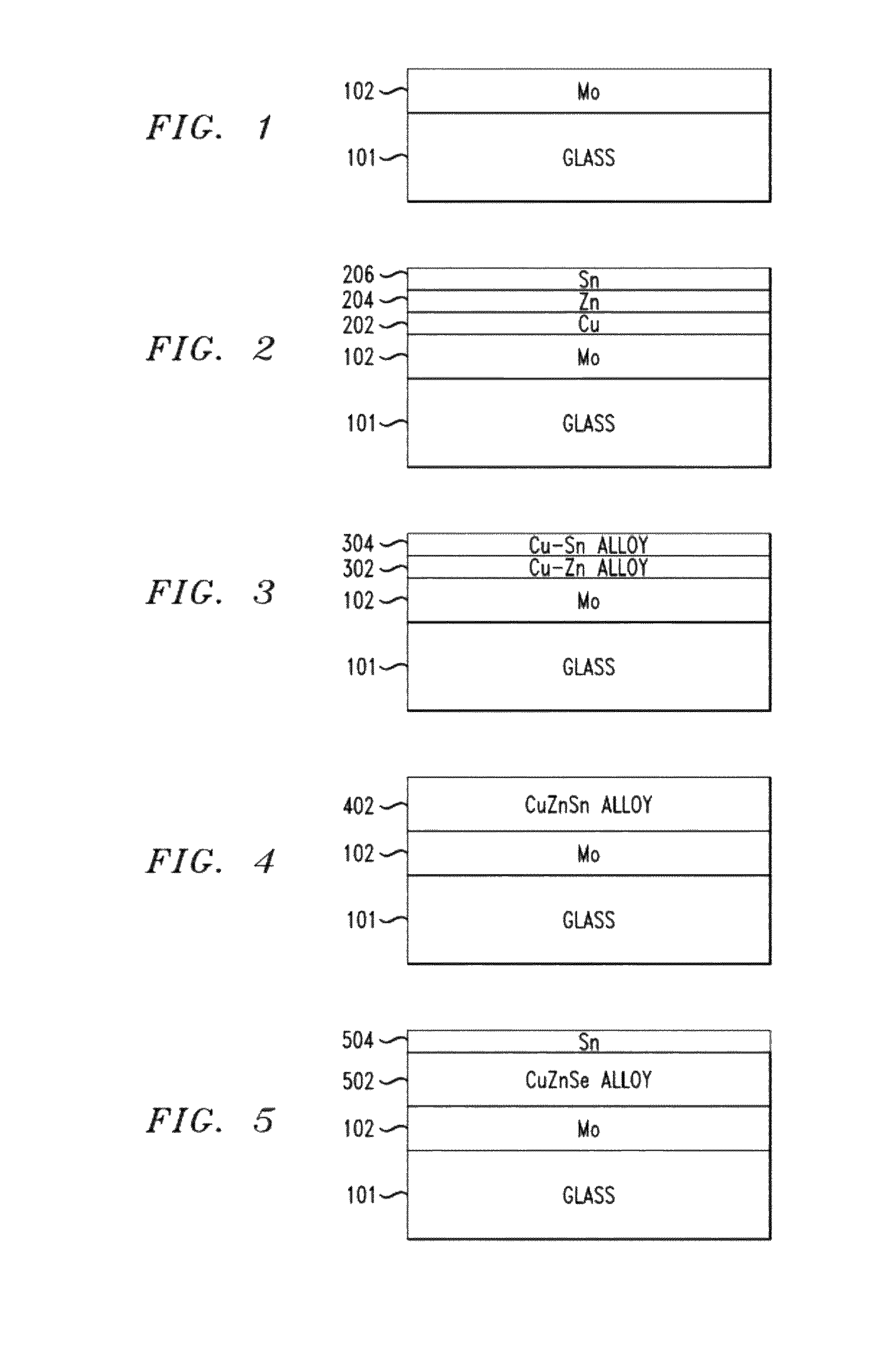
[0033]FIGS. 1-10 are cross-sectional diagrams illustrating an exemplary methodology for fabricating a diode, e.g., a solar cell. To begin the fabrication process, a substrate 101 is provided. Suitable substrates include, but are not limited to, glass, metal, metal foil, stainless steel and copper (Cu) foil substrates. A backside electrode 102 is then formed on the substrate. Suitable materials for forming the backside electrode include, but are not limited to, molybdenum (Mo), Cu and titanium (Ti). The backside electrode material may be deposited on the substrate using a physical vapor deposition (PVD) method. A metal (e.g., Cu) layer (not shown) may be present on the b...


PUM

PropertyMeasurementUnit
temperatureaaaaaaaaaa

Abstract

Techniques for using electrodeposition to form absorber layers in diodes (e.g., solar cells) are provided. In one aspect, a method for fabricating a diode is provided. The method includes the following steps. A substrate is provided. A backside electrode is formed on the substrate. One or more layers are electrodeposited on the backside electrode, wherein at least one of the layers comprises copper, at least one of the layers comprises zinc and at least one of the layers comprises tin. The layers are annealed in an environment containing a sulfur source to form a p-type CZTS absorber layer on the backside electrode. An n-type semiconductor layer is formed on the CZTS absorber layer. A transparent conductive layer is formed on the n-type semiconductor layer. A diode is also provided.

Description

FIELD OF THE INVENTION[0001]The present invention relates to electrodeposition fabrication processes and more particularly, to techniques for using electrodeposition to form absorber layers in diodes (e.g., solar cells).BACKGROUND OF THE INVENTION[0002]Low-cost, earth abundant materials, such as Cu2ZnSn(S,Se)4 (CZTS), have been developed as an alternative to higher cost, less available copper indium gallium selenide (CIGS) absorber materials for next generation thin film photovoltaic devices. CZTS is one of the most promising materials for fabricating low-cost thin film solar cells. CZTS consists of earth abundant materials like copper (Cu), zinc (Zn) and tin (Sn) and has band gap energy of from 1.4 electron volt (eV) to 1.5 eV and an absorption co-efficient of 104 cm−1. See, for example, Hideaki Araki et al, “Preparation of Cu2ZnSnS4 Thin Films by Sulfurizing Electroplated Precursors,” Solar Energy Materials & Solar Cells, 93, 996-999 (2009), P. M. P Salome et al., “Influence of Se...

Claims


Application Information

Patent Timeline
Patent Type & Authority Patents(United States)
IPC IPC(8): H01L23/482
CPCC25D5/10C25D5/50H01L21/02422H01L21/02491H01L21/02568H01L21/02614H01L31/0326H01L31/072H01L31/0272H01L31/0224H01L31/18H01L21/02628Y02E10/50H01L2924/10822C25D5/611C25D5/619
Inventor AHMED, SHAFAATDELIGIANNI, HARIKLIAROMANKIW, LUBOMYR T.WANG, KEJIA
Owner GLOBALFOUNDRIES INC
Why Eureka
Try Eureka