

Semiconductor device mounted structure and its manufacturing method, semiconductor device mounting method, and pressing tool
a semiconductor and mounting technology, applied in the direction of manufacturing tools, soldering devices, auxillary welding devices, etc., can solve the problems of cracks or peeling after mounting, large stress loads at portions of semiconductor chips, and more fragile mechanical strength of insulation materials, so as to avoid internal breakdown of semiconductor device mounting structures
- Summary
- Abstract
- Description
- Claims
- Application Information
AI Technical Summary
Benefits of technology
Problems solved by technology
Method used
Image

Examples
first embodiment
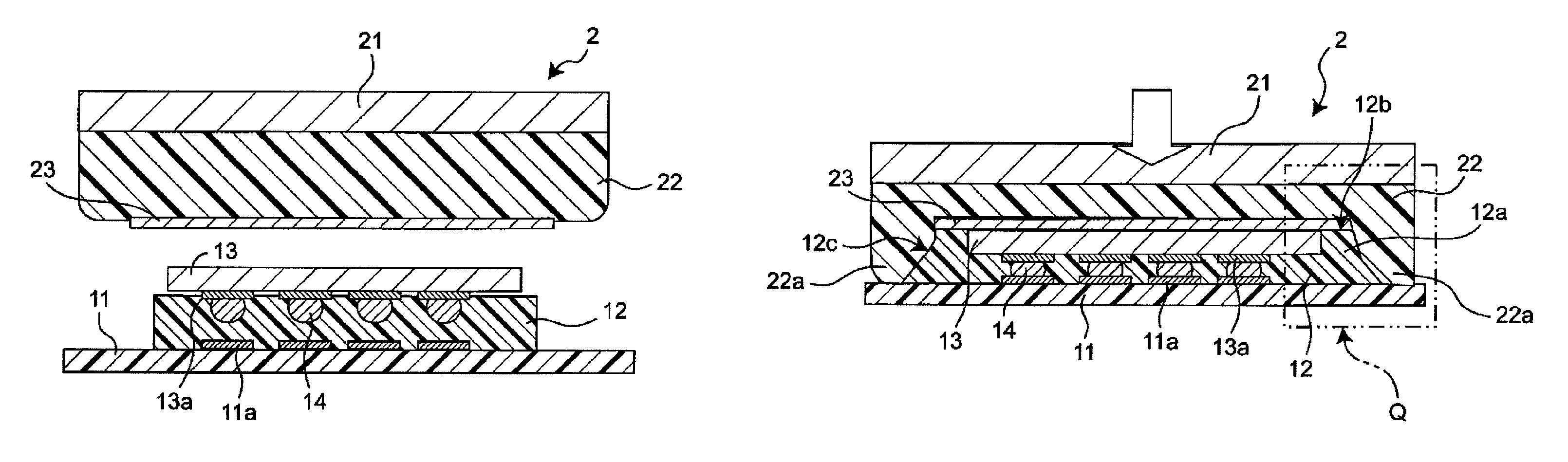
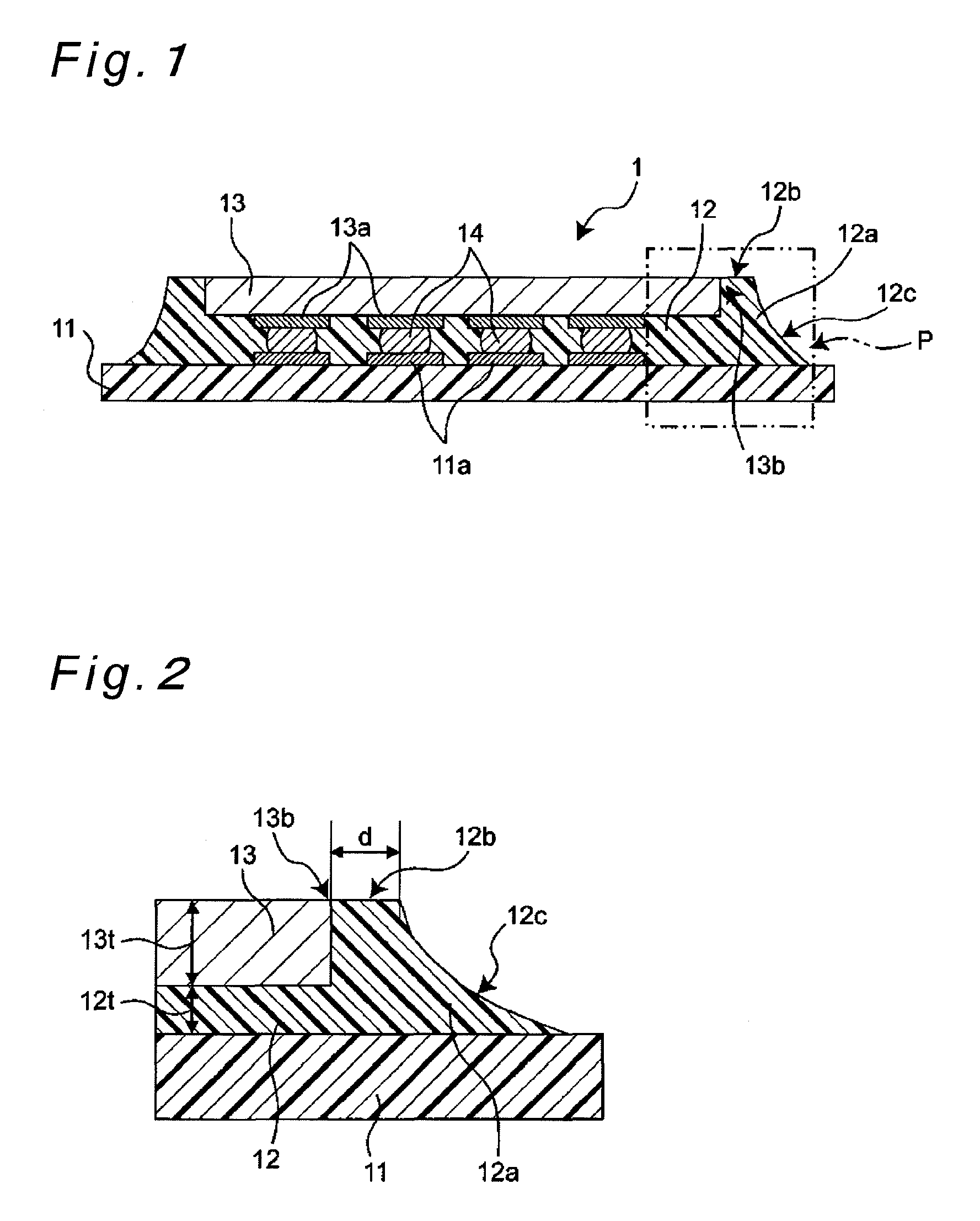
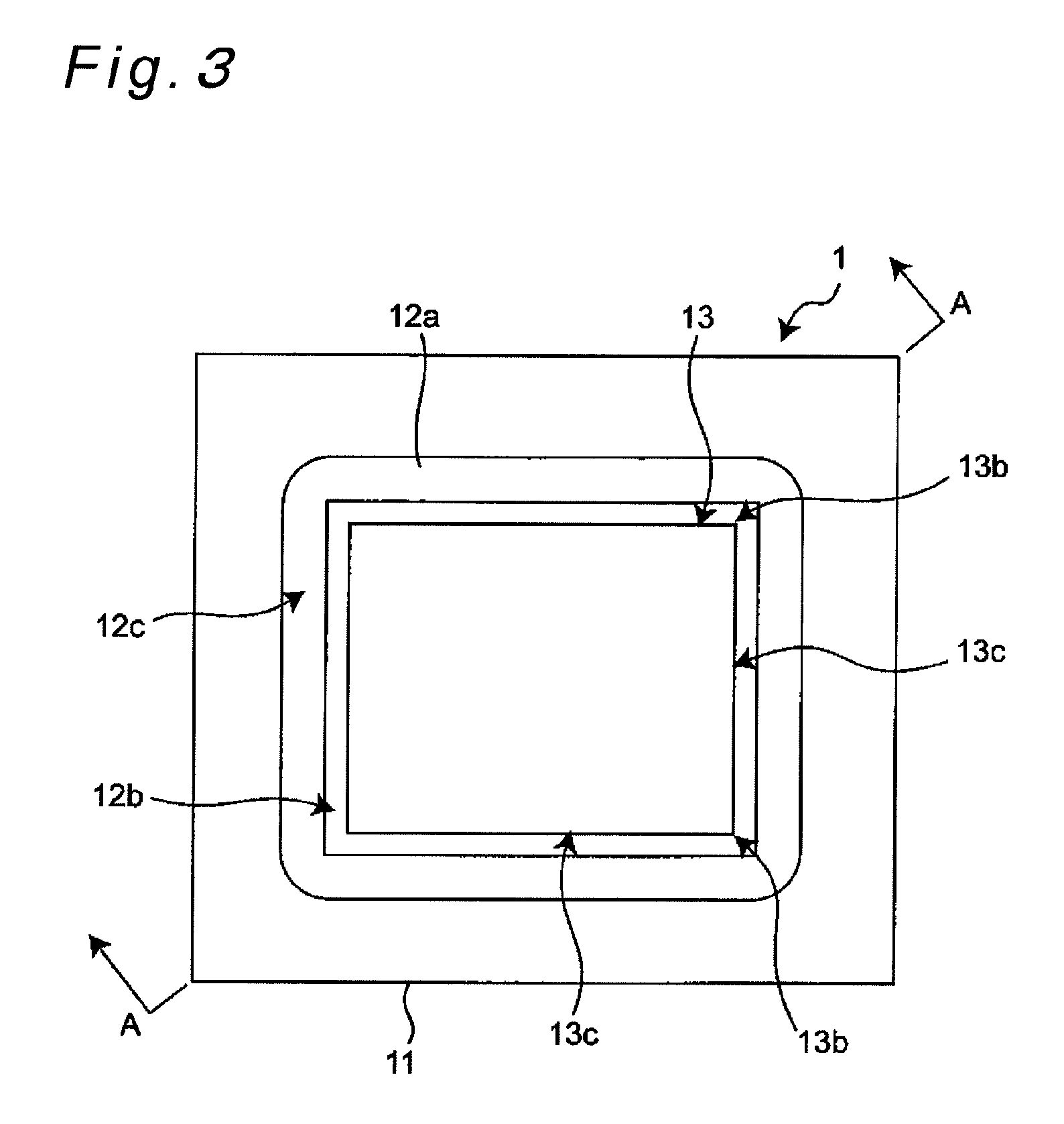
[0068]FIG. 1 shows a schematic sectional view of a semiconductor chip mounted structure 1 which is an example of a semiconductor device mounted structure according to a first embodiment of the invention. FIG. 2 is an enlarged schematic sectional view of a portion P of the mounted structure 1 of FIG. 1, and FIG. 3 is a schematic plan view of the mounted structure 1. In addition, FIG. 1 is a sectional view taken along the line A-A of FIG. 3.
[0069]As shown in FIGS. 1 and 3, in the semiconductor chip mounted structure 1 of this first embodiment, a sealing resin (e.g., sheet-like underfill) 12 as an example of the seal-bonding resin is set on a board 11, and a semiconductor chip 13 is mounted via the sealing resin 12. A plurality of pads 13a as an example of device electrodes are formed on a circuit formation surface, lower-side surface in the figure, of the semiconductor chip 13. In correspondence to formation positions of these pads 13a, a plurality of board electrodes 11a are formed o...
second embodiment
[0093]The present invention may be carried out in other various modes without being limited to the above embodiment. For example, a semiconductor chip mounted structure manufacturing method according to a second embodiment of the invention is described with reference to the schematic sectional views of FIGS. 11, 12 and 13. In addition, FIG. 13 is an enlarged partial schematic sectional view of a portion R in FIG. 12.
[0094]As shown in FIGS. 11 and 12, in the manufacturing method of the second embodiment, a tool 3 different in structure from the tool 2 of the first embodiment is used. The tool 3 includes a tool body portion 31 as an example of the pressing member having, at its lower surface, a pressing surface 31a for the semiconductor chip 13, and an elastic member 32 placed all around the pressing surface 31a of the tool body portion 31 so as to surround the pressing surface 31a. The pressing surface 31a of the tool body portion 31 is formed larger than the planar outer shape of th...
third embodiment
[0098]Next, FIG. 14 is a schematic plan view of a semiconductor chip mounted structure 4 according to a third embodiment of the invention.
[0099]As shown in FIG. 14, the mounted structure 4 of the third embodiment differs from the foregoing first and second embodiments in that a fillet portion 42a is formed so as to be relatively larger in resin amount at vicinities of corner portions 13b of a semiconductor chip 13 where stress caused by thermal contraction and the like of the board 11 or the like is more likely to be concentrated. In the mounted structure 4 of such a structure, since the corner portions 13b are protected enough, internal breakdown of the semiconductor chip 13 can be prevented further effectively.
[0100]The fillet portion 42a of such a structure can be formed by using, for example, a tool 5 shown in the schematic plan view of FIG. 15. More specifically, as shown in FIG. 15, the tool 5 includes a tool body portion and an elastic member 22 similar to those of the first ...
PUM
 Abstract
Description
Claims
Application Information