Substrate structure for plasma display panel, method of manufacturing the substrate structure, and plasma display panel including the substrate structure

a substrate structure and plasma display technology, applied in the field of plasma display, can solve the problems of higher voltage drop, more power consumption, pdp to run at a slower rate, etc., and achieve the effect of simplifying the manufacturing process, low specific resistance, and low specific resistan

Inactive Publication Date: 2013-05-07
SAMSUNG SDI CO LTD
View PDF45 Cites 2 Cited by
  • Summary
  • Abstract
  • Description
  • Claims
  • Application Information

AI Technical Summary

Benefits of technology

[0013]According to an embodiment of the present invention, an electrode (e.g., a bus electrode for a PDP) includes a first layer and a second layer. The second layer is formed on a substrate and includes an aluminum (Al) material. The first layer is formed between the substrate and the second layer and includes a conductive material having lower specific resistance than that of Al. A light absorbable layer is formed on the substrate and adjacent to the electrode, the light absorbable layer being an oxidization product of the conductive material of the first layer. As such, the electrode includes Al that is relatively inexpensive, not a noble metal, and can be formed using a photolithographic method that does not require an expensive apparatus; and, at the same time, the electrode can have a relatively low specific resistance (e.g., about 20 μΩ·cm or less).
[0014]Also, in one embodiment, the second layer further includes a surface treatment agent that protects the Al material from oxidation. Furthermore, in one embodiment, the first layer formed into the electrode also has a portion extending out from the electrode that is oxidized to form the light absorbable layer, thereby simplifying the manufacturing process.

Problems solved by technology

The high resistant electrodes may cause the PDP to run at a slower rate, with higher voltage drop and / or with more power consumption.

Method used


Image

  • Substrate structure for plasma display panel, method of manufacturing the substrate structure, and plasma display panel including the substrate structure
  • Substrate structure for plasma display panel, method of manufacturing the substrate structure, and plasma display panel including the substrate structure
  • Substrate structure for plasma display panel, method of manufacturing the substrate structure, and plasma display panel including the substrate structure

Examples


Embodiment Construction

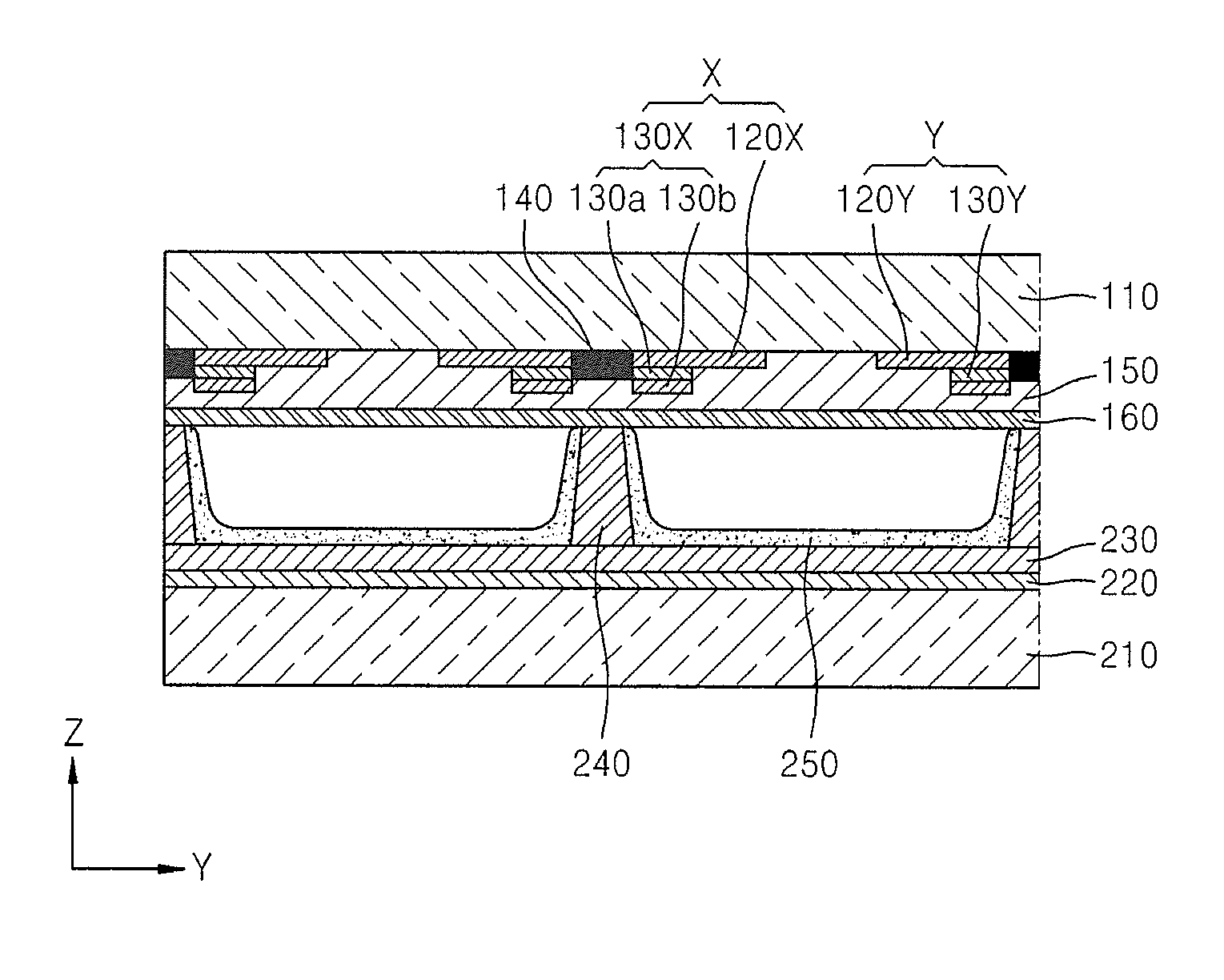
[0032]In the following detailed description, only certain exemplary embodiments of the present invention are shown and described, by way of illustration. As those skilled in the art would recognize, the invention may be embodied in many different forms and should not be construed as being limited to the embodiments set forth herein. Also, in the context of the present application, when an element is referred to as being “on” another element, it can be directly on another element or be indirectly on another element with one or more intervening elements interposed therebetween. Like reference numerals designate like elements throughout the specification.

[0033]Hereinafter, a substrate structure for a plasma display panel (PDP), a method of manufacturing a PDP substrate structure of the PDP, and a PDP including the PDP substrate structure will be described in more detail with reference to the accompanying drawings, in which exemplary embodiments of the invention are shown.
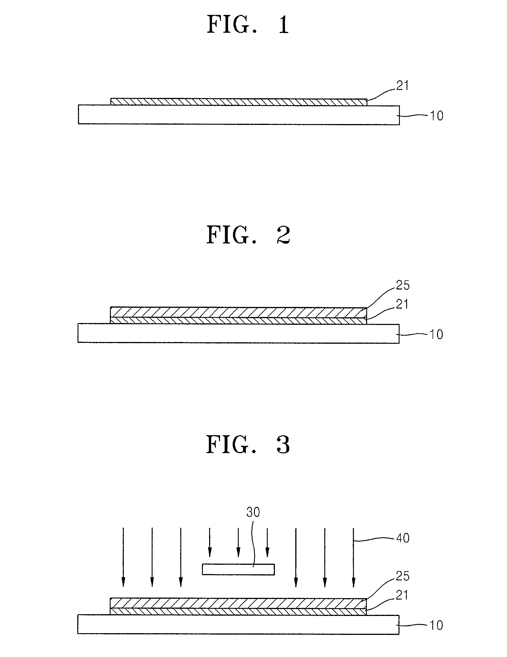
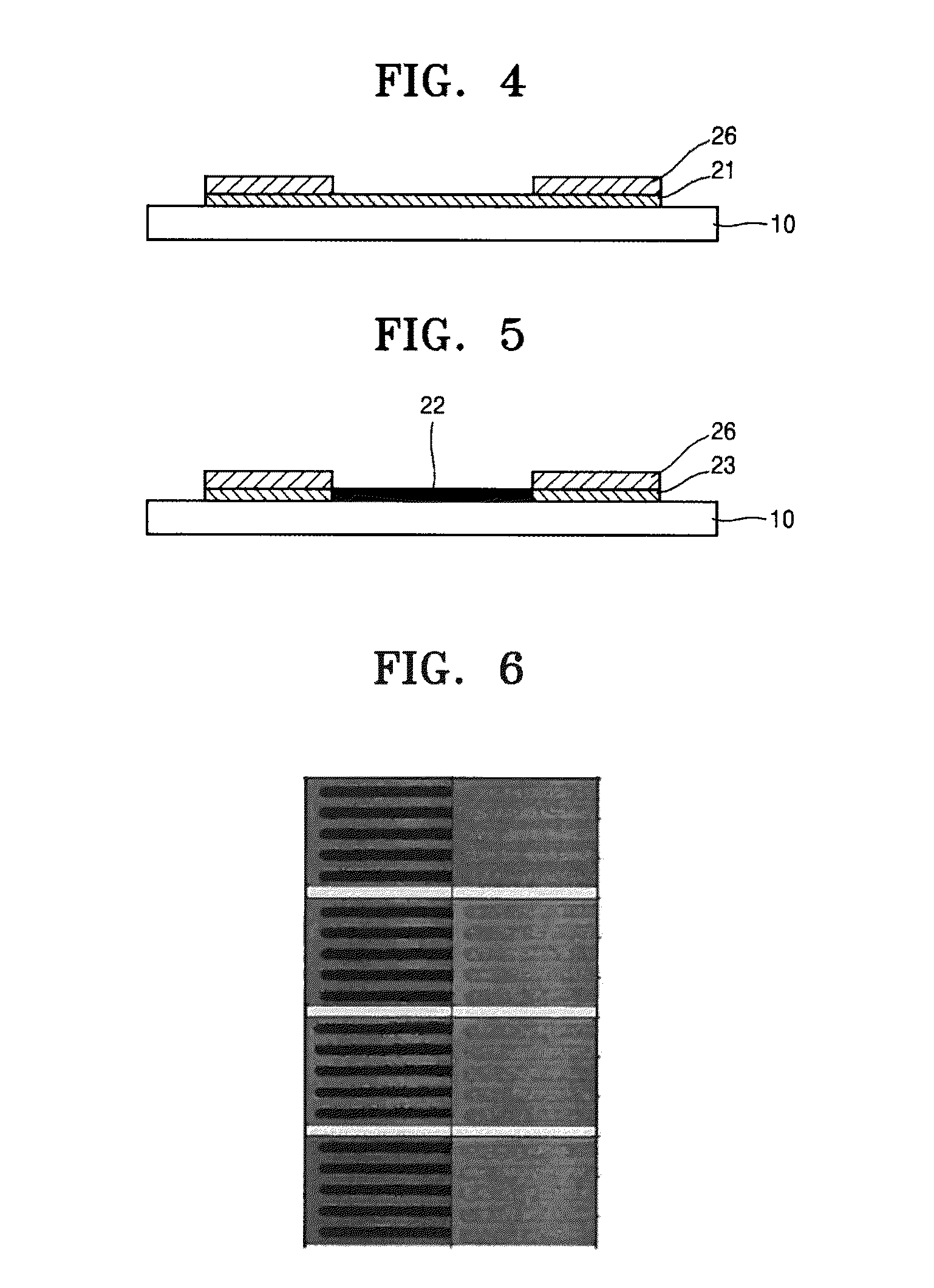
[0034]A method...


PUM

PropertyMeasurementUnit
particle radiusaaaaaaaaaa
radiusaaaaaaaaaa
average radiusaaaaaaaaaa

Abstract

A substrate structure for a plasma display panel (PDP), a method of manufacturing a PDP substrate structure of the PDP, and a PDP including the PDP substrate are provided. The PDP substrate structure includes a substrate, an electrode on the substrate and including a first layer and a second layer, the second layer including an aluminum (Al) material, the first layer being between the substrate and the second layer and including a conductive material, the first layer having lower specific resistance than that of the second layer; and a light absorbable layer on the substrate. The light absorbable layer is an oxidization product of the conductive material of the first layer.

Description

CROSS-REFERENCE TO RELATED APPLICATIONS[0001]This application claims priority to and the benefit of U.S. Provisional Patent Application Nos. 61 / 078,730 and 61 / 078,722, both filed on Jul. 7, 2008, in the United States Patent and Trademark Office, the entire contents of which are incorporated herein by reference.BACKGROUND[0002]1. Field of the Invention[0003]The present invention relates to a plasma display (PDP) and, more particularly, to a PDP substrate structure of the PDP and its manufacturing method.[0004]2. Description of the Related Art[0005]A plasma display panel (PDP) is a display device for realizing an image by gas discharge. That is, the gas discharge generates plasma, the plasma radiates vacuum ultraviolet (VUV) rays, the VUV rays excite phosphors, and the excited phosphors are stabilized to generate red (R), green (G), and blue (B) visible light.[0006]For example, in one type of PDP, address electrodes are formed on a first (or rear) substrate, and a dielectric layer is ...

Claims


Application Information

Patent Timeline
Patent Type & Authority Patents(United States)
IPC IPC(8): H01J17/49
CPCH01J9/02H01J9/2278H01J11/12H01J11/44H01J2211/225H01J2211/444
Inventor KIM, CHUL-HONGKIM, MIN-JAECHAE, SO-RAHEO, EUN-GI
Owner SAMSUNG SDI CO LTD
Why Eureka
Try Eureka