Memory device and manufacturing method of the same

a technology of memory and manufacturing method, which is applied in the direction of semiconductor devices, semiconductor/solid-state device details, instruments, etc., can solve the problems of increasing the size of the completed device, increasing the cost of manufacturing two circuits that are a memory and other functional circuits, and reducing the efficiency of manufacturing, so as to reduce the cost of manufacturing, not limit the product specifications, and reduce the effect of productivity

Inactive Publication Date: 2012-02-14
SEMICON ENERGY LAB CO LTD
View PDF33 Cites 2 Cited by
  • Summary
  • Abstract
  • Description
  • Claims
  • Application Information

AI Technical Summary

Benefits of technology

[0013]It is difficult to form a nonvolatile memory and other functional circuits on the same substrate with conventional technologies, regardless of whether a semiconductor integrated circuit is formed on a silicon substrate or an insulating substrate. However, when a memory and other functional circuits are formed separately to obtain one device, they are required to be connected externally, which results in increased size of a completed device. In addition, at least two circuits that are a memory and other functional circuits are expensive to manufacture. Even when a memory and other functional circuits can be formed on the same substrate as a flash memory and a ferroelectric memory, additional steps are required to form the memory. In the manufacture of a semiconductor device, increase in manufacturing steps leads to high cost, limits product specifications, and decreases productivity.
[0015]In view of the foregoing, the invention provides a manufacturing method of a write-once memory that can be formed by TFT manufacturing steps similarly to other functional circuits formed on an insulating substrate. Further, the invention provides an easy-to-use and inexpensive memory device while maintaining product specifications and productivity even when a memory is formed on the same substrate as other functional circuit.
[0022]According to the aforementioned structures, a write-once memory can be formed on an insulating substrate by TFT manufacturing steps. That is, the memory device of the invention can be formed by TFT manufacturing steps similarly to other functional circuits formed on an insulating substrate, which can suppress an increase in extra cost due to additional manufacturing steps of a memory. In addition, since a memory and other functional circuits can be formed by the same steps, the memory does not limit product specifications and not decrease productivity.
[0023]A glass substrate and a plastic substrate are quite inexpensive as compared to a silicon substrate. Further, it is possible to use an insulating substrate with a larger area than a silicon substrate that is limited to a small area. Thus, the number of products manufactured on an insulating substrate increases than that manufactured on a silicon substrate, leading to a very inexpensive semiconductor device.
[0024]According to the invention, a write-once memory is formed by TFT manufacturing steps, thereby an easy-to-use and inexpensive memory device can be provided while maintaining product specifications and productivity even when a memory is formed on the same substrate as other functional circuit.

Problems solved by technology

It is difficult to form a nonvolatile memory and other functional circuits on the same substrate with conventional technologies, regardless of whether a semiconductor integrated circuit is formed on a silicon substrate or an insulating substrate.
However, when a memory and other functional circuits are formed separately to obtain one device, they are required to be connected externally, which results in increased size of a completed device.
In addition, at least two circuits that are a memory and other functional circuits are expensive to manufacture.
In the manufacture of a semiconductor device, increase in manufacturing steps leads to high cost, limits product specifications, and decreases productivity.
Accordingly, they cannot be formed on the same substrate as other functional circuits or they require additional steps other than TFT manufacturing steps even when formed on the same substrate as other functional circuits.
Such a problem leads to extra cost for a memory in the manufacture of a semiconductor device having a function, for example such as an IC tag.

Method used


Image

  • Memory device and manufacturing method of the same
  • Memory device and manufacturing method of the same
  • Memory device and manufacturing method of the same

Examples


embodiment mode 1

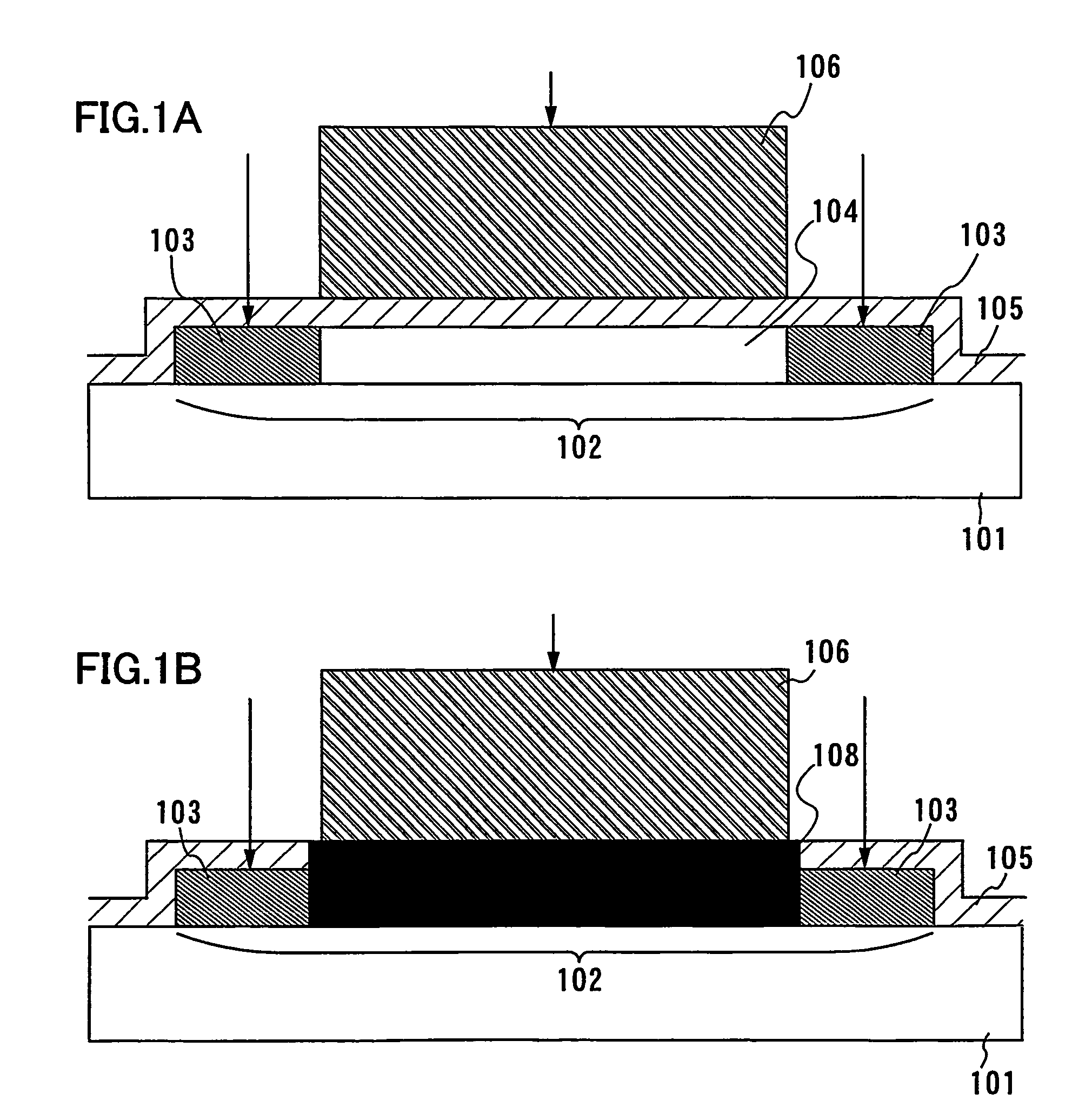
[0036]When a voltage higher than required for normal operation of a TFT is applied between a gate electrode and at least one of two impurity regions (including a high concentration impurity region) of the TFT formed on an insulating substrate, a channel region of the TFT is insulated. This operation is shown in FIGS. 1A and 1B that are cross sectional views of a TFT before and after being applied a voltage respectively. For example, a TFT shown in FIG. 1A has a semiconductor film 102 formed over an insulating substrate 101, a gate insulating film 105 over the semiconductor film 102, and a gate electrode 106 over the gate insulating film 105. The semiconductor film 102 includes two high concentration impurity regions 103 and a channel region 104. FIG. 1B shows the TFT after being applied a voltage. In the TFT, at least the channel region 104 of the semiconductor film 102 is altered and an insulating region 108 is formed under the gate electrode 106. Then, the gate electrode 106 and t...

embodiment mode 2

[0050]In a memory device of the invention, a high concentration impurity may be added over the entire surface of a semiconductor film of TFT as a memory cell. Instead, an impurity may be added to any portion of a semiconductor film and two wirings may be connected thereto; however, when forming an impurity region arbitrarily, the element does not function as a transistor. Meanwhile, when a high concentration impurity is added over the entire surface of a semiconductor film, all the three terminals can be insulated from each other by applying a voltage between an electrode and at least one of two wirings.

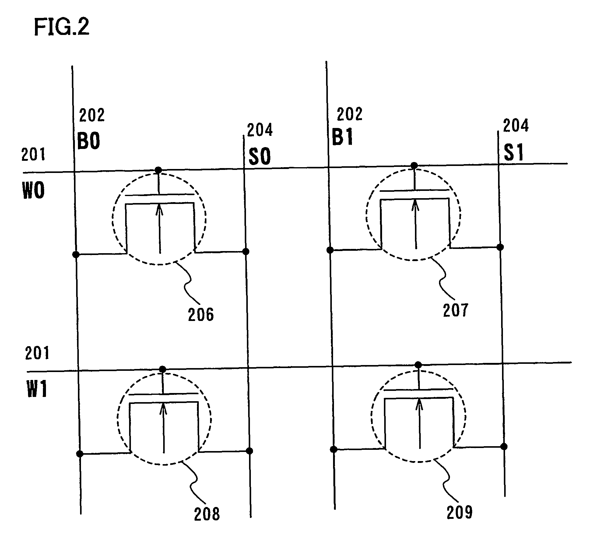
[0051]Described in this embodiment mode is an example where one impurity region (high concentration impurity region in this embodiment mode) is formed over a semiconductor film on an insulating substrate and two wirings are connected to the semiconductor film with one electrode interposed therebetween. FIGS. 3A and 3C are top plan views of an element having such a structure. FIGS. 3B...

embodiment

Embodiment 1

[0061]In this embodiment, a manufacturing method of a TFT on a glass substrate is specifically described with reference to FIGS. 5A to 5E, FIGS. 6A to 6D and FIGS. 7A and 7B. Description is made with reference to cross sectional views of an N-channel TFT and a P-channel TFT.

[0062]First, a peeling layer 501 is formed over a substrate 500 (FIG. 5A). In this embodiment, an a-Si film (amorphous silicon film) with a thickness of 50 nm is formed over a glass substrate (e.g., a 1737 substrate, product of Corning Incorporated) by low pressure CVD. As for the substrate 500, a quartz substrate, a substrate made of an insulating material such as alumina, a silicon wafer substrate, a plastic substrate having enough heat resistance to the treatment temperature in the subsequent step, and the like may be employed as well as the glass substrate. The peeling layer 501 is preferably formed of a film mainly containing silicon such as polycrystalline silicon, single crystalline silicon and...


PUM


Abstract

An easy-to-use and inexpensive memory device is provided while maintaining product specifications and productivity even when a memory is formed on the same substrate as other functional circuits. The memory device of the invention includes a memory cell formed on an insulating surface. The memory cell includes a semiconductor film having two impurity regions, a gate electrode, and two wirings connected to the respective impurity regions. The two wirings are insulated from each other by applying a voltage between the gate electrode and at least one of the two wirings to alter the state of the semiconductor film.

Description

TECHNICAL FIELD[0001]The present invention relates to a memory device, and more particularly to a nonvolatile memory device.BACKGROUND ART[0002]In modern society, many electronic appliances are used and various data is generated and employed, requiring a memory device to store the data. Various memory devices produced and used today each has different advantages and disadvantages, and is selected depending on the data to be stored and used.[0003]For example, a volatile memory that loses its memory content when the power is turned off includes a DRAM and an SRAM. The volatile memory has limited applications because of the volatility; however, it is used as a main memory device or a cash memory of a computer taking advantage of a short access time. As each memory cell has a small size, a large-capacity DRAM can be produced easily, though it is controlled in a complex manner and consumes much power. Meanwhile, an SRAM includes a memory cell constituted by a CMOS and is easily manufactu...

Claims


Application Information

Patent Timeline
Patent Type & Authority Patents(United States)
IPC IPC(8): H01L27/12H01L21/336G11C17/16H01L21/77H01L21/82H01L21/8246H01L21/8247H01L21/84H01L27/10H01L27/115H01L29/786
CPCG11C17/16H01L27/112H01L27/115H01L27/11517H01L27/1203H10B20/00H10B41/00H10B69/00
Inventor KATO, KIYOSHIYAMAGUCHI, TETSUJIASANO, ETSUKOIZUMI, KONAMI
Owner SEMICON ENERGY LAB CO LTD
Why Eureka
Try Eureka