Optical module

a technology of optical modules and optical modules, applied in the field of optical modules, can solve the problems of deterioration of transmission characteristics, easy reduction of transmission characteristics, and change of characteristic impedance, and achieve the effects of excellent transmission characteristics, easy acquisition of optical modules, and easy deterioration of high-frequency signals

Active Publication Date: 2013-05-07
LUMENTUM JAPAN INC
View PDF22 Cites 18 Cited by
  • Summary
  • Abstract
  • Description
  • Claims
  • Application Information

AI Technical Summary

Benefits of technology

[0012]In the manufacturing steps of the flexible substrate, the patterning of the conductor pattern of the surface and the conductor pattern of the back surface cannot be carried out at the same time. Generally, the conductor patterns are separately pasted onto a base film, or the patterning is carried out by separately subjecting the surface and the back surface to etching. In such cases, generally, positional misalignment of up to about 50 microns is caused between the conductor pattern of the surface and the conductor pattern of the back surface. If an attempt to eliminate the positional misalignment is made, productivity is significantly lowered. When this flexible substrate is used in external connection of the package of the optical module, an examination of the flexible substrate is required in advance. Therefore, if the structure does not readily affect the characteristics as a result of arrangement of the conductor layout of the flexible substrate, even when the positional misalignment of the surface / back surface conductor patterns is generated, such an examination step is no longer required to be carried out.
[0015]Thus, not only deterioration of high-frequency signals due to the shift in the characteristic impedance, but also deterioration of the high-frequency signals due to radiation of electromagnetic waves (noise) is caused. An optical transceiver using such an optical module readily causes operation failure.
[0017]In this manner, in the optical module using the conventional flexible substrate, characteristic deterioration of high-frequency signals is readily caused, and an examination of the flexible substrate has been inevitable in advance in order to prevent it.
[0018]The present invention has been accomplished in order to solve the above-described problems of the conventional techniques, and it is a preferred aim of the present invention to provide techniques capable of readily obtaining an optical module having excellent transmission characteristics.
[0023]If the electromagnetic field of the surface ground line and the signal line is dominant at the point where the grounded coplanar line is switched to the coplanar line, conversion of the electromagnetic field distribution is smoothly carried out, and the influence exerted on the characteristics of the flexible substrate by the positional misalignment of the conductor patterns of the surface and the back surface is extremely small. Therefore, the parts examination which is carried out in order to suppress defects caused by the positional misalignment before the flexible substrate is connected to the lead pins can be simplified, and yield can be maintained to be high even without the parts examination. Moreover, since the impedance is not shifted, an optical module having small noise and excellent high-frequency transmission characteristics can be manufactured at a low cost with good reproducibility.
[0027]According to the present invention, an optical module having excellent high-frequency transmission characteristics can be provided at a low cost.

Problems solved by technology

The flexible substrate disclosed in above-described Patent Document 1 has a problem that reduction in transmission characteristics is readily caused due to the positional misalignment caused in a process described below.
Therefore, there has been a possibility that the characteristic impedance may be changed and deterioration in the transmission characteristics may be caused.

Method used


Image

  • Optical module
  • Optical module
  • Optical module

Examples


first embodiment

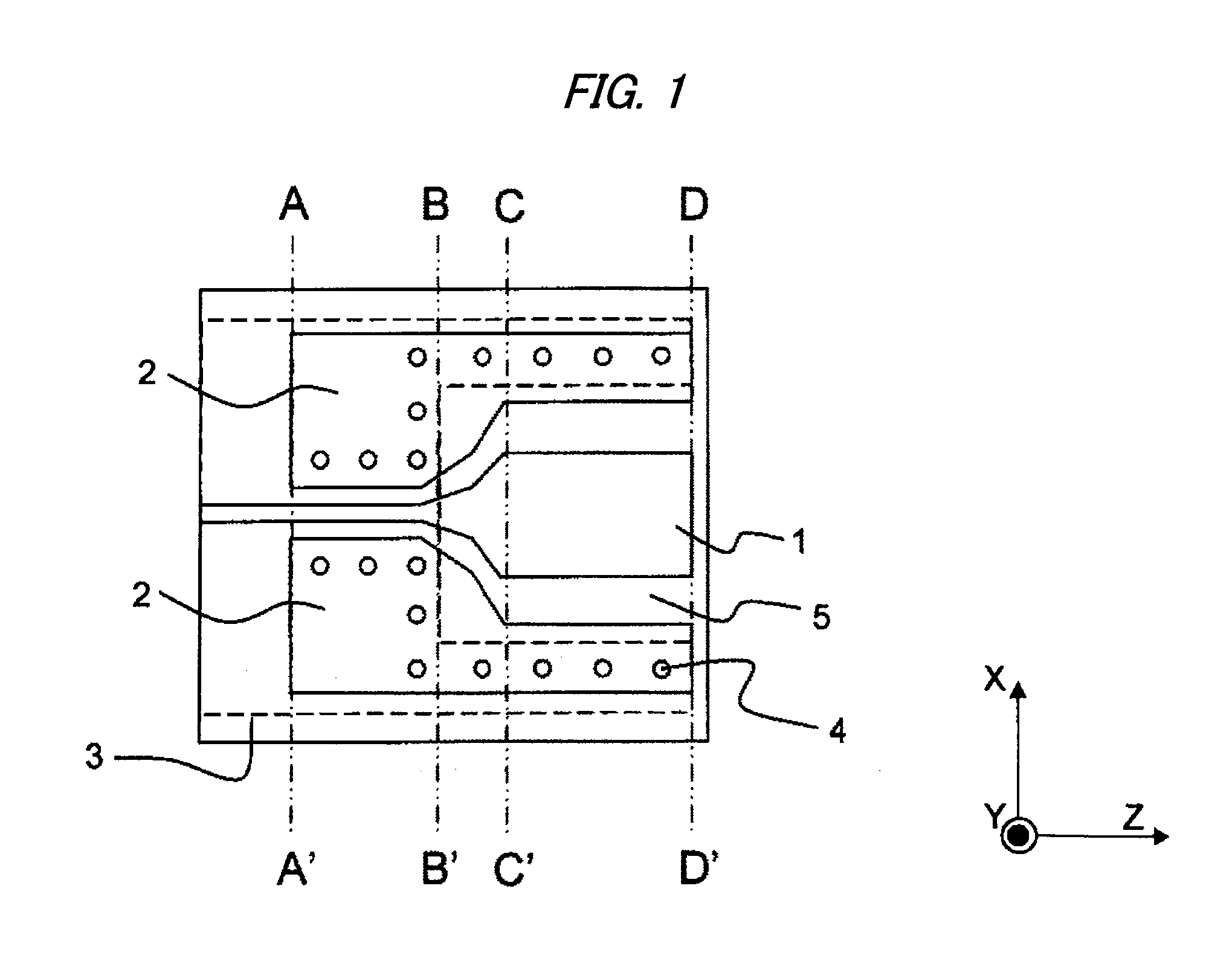
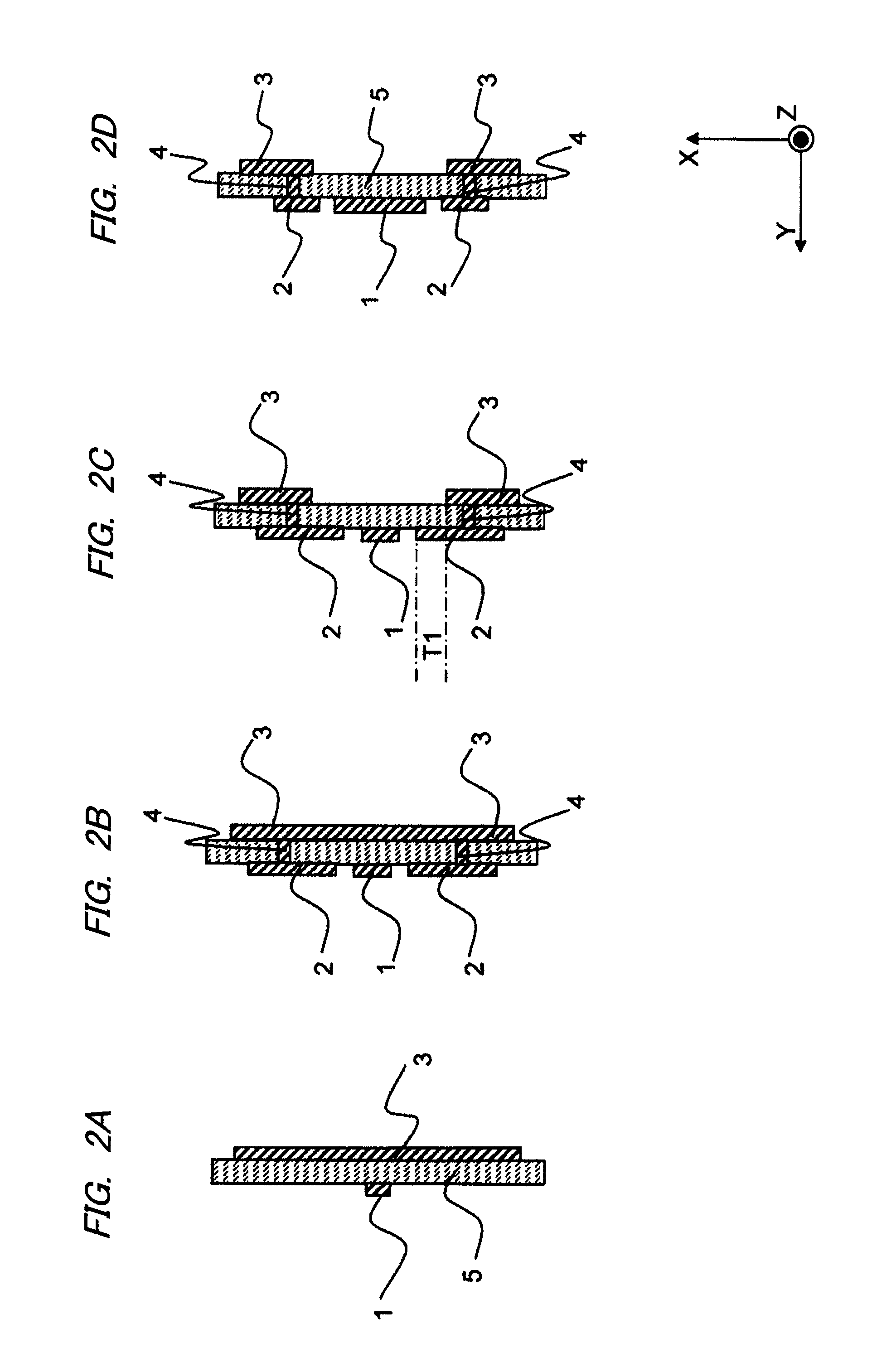
[0051]FIG. 1 is a top view showing a configuration of a flexible substrate of a first embodiment. FIG. 2A to FIG. 2D illustrate a cross-sectional view of the left side of A-A′ of FIG. 1, a cross-sectional view of the part between A-A′ and B-B′, a cross-sectional view of the part between B-B′ and C-C′, and a cross-sectional view of the part between C-C′ and D-D′, respectively.

[0052]In FIG. 1 and later-described FIGS. 3-5, 6, 8, 10 and 13, wiring patterns formed on a surface (upper surface) side of a base film 5 are illustrated by solid lines, and wiring patterns formed on aback surface side are illustrated by dotted lines. Hereinafter, these electrode layout patterns will be described.

[0053]As is understood from FIG. 2A to FIG. 2D, a signal line 1 to which signals representing information to be transmitted are applied and surface ground lines 2 to which a ground potential is applied are patterned on the surface side of the base film 5, and a back-surface ground line 3 to which the gr...

second embodiment

[0072]FIG. 3 is a top view illustrating a configuration of a flexible substrate of a second embodiment of the present invention, and FIG. 4 is a top view illustrating a configuration of a modification example of the flexible substrate of the second embodiment of the present invention.

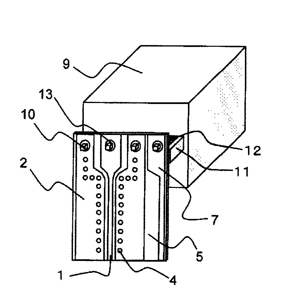
[0073]FIG. 3 and FIG. 1 have two different points. The first different point is that a signal pad 6 connected by contact holes 4 are patterned on the back surface that is overlapped with the signal line 1 in the coplanar line. A lead pin can be fixedly attached by the signal pad 6 from the back-surface side of the flexible substrate.

[0074]A width L3 of the signal pad 6 is narrower than a width L4 of the coplanar line of the signal line 1. In other words, the signal line 1 of the surface side is closer to the ground lines 2 than the signal pad 6 of the back-surface side is. Thus, there are advantages that the influence exerted on the characteristic impedance by the signal pad 6, which is patterned on the...

third embodiment

[0077]FIG. 5 is a top view showing a configuration of a flexible substrate of a third embodiment of the present invention.

[0078]A point largely changed from FIG. 1 is that the back-surface ground line 3 is not provided in the coplanar line. The characteristic impedance of this part is maintained substantially only by the distances between the signal line 1 and the surface ground lines 2. This case has an advantage that a variation in the characteristic impedance due to the surface / back surface pattern positional misalignment in the X-axis direction is almost completely eliminated even when the positional misalignment of the surface / back surface patterns of the flexible substrate is particularly large.


PUM


Abstract

An optical module having a flexible substrate having, even after actual manufacturing steps, excellent transmission characteristics of high-frequency signals and an advantage that electromagnetic field radiation is reduced even when it is connected with a package. The flexible substrate used in external connection of the package of the optical module uses a flexible substrate having a coplanar line to which a lead pin is fixedly attached, a grounded coplanar line which is in contact with the coplanar region, and a microstrip line which is in contact with the grounded coplanar line. The flexible substrate has an electrode layout in which an electromagnetic field component of a surface ground line and a signal line is more dominant than an electromagnetic field component of a back-surface ground line and the signal line in a region of the coplanar line adjacent to the grounded coplanar line.

Description

CROSS-REFERENCE TO RELATED APPLICATION[0001]The present application claims priority from Japanese Patent Application No. JP 2009-037710 filed on Feb. 20, 2009, the content of which is hereby incorporated by reference into this application.TECHNICAL FIELD OF THE INVENTION[0002]The present invention relates to an optical module and particularly relates to a flexible substrate and an optical module in which lead pins of a package (module housing for mounting optical elements) are fixedly attached to the flexible substrate.BACKGROUND OF THE INVENTION[0003]An optical communication network is composed of optical fibers serving as media for propagating optical signals and optical transceivers for transmitting / receiving optical signals. A housing of the optical transceiver encloses an optical module for converting electric signals to optical signals and optical signals to electric signals and a printed board on which electronic elements and electric connectors, etc. are mounted for control....

Claims


Application Information

Patent Timeline
Patent Type & Authority Patents(United States)
IPC IPC(8): G02B6/12G02B6/26
CPCG02B6/4201H05K1/0219G02B6/4246H05K2201/09618H05K1/118H05K1/147H05K3/361H05K1/0253G02B6/424G02B6/4244G02B6/4251G02B6/4281G02B6/4283
Inventor BAN, TAKUMA
Owner LUMENTUM JAPAN INC
Why Eureka
Try Eureka