Semiconductor light emitting device having an optical plate including a meniscus control structure and method of manufacturing

a technology of light-emitting devices and optical plates, which is applied in the direction of discharge tubes/lamp details, luminescnet screens, lighting and heating apparatus, etc., can solve the problems of difficult to reduce the size of light-emitting surfaces, difficult to lead frame light-emitting devices, etc., and achieve high light-emitting efficiency

Active Publication Date: 2013-06-04
STANLEY ELECTRIC CO LTD
View PDF23 Cites 9 Cited by
  • Summary
  • Abstract
  • Description
  • Claims
  • Application Information

AI Technical Summary

Benefits of technology

[0029]In the above-described exemplary semiconductor light-emitting device, the convex shape of the meniscus control structure can be located between the bottom surface of the optical plate and an extended surface of each top surface of the adjacent light-emitting chips in order to reduce color variability of light emitted from the device. The device can further include an outer meniscus control structure projecting from the bottom surface of the optical plate toward the light-emitting chips and extending along the edge of the optical plate so as to easily be able to form various light-emitting surfaces, and also can further a particulate spacer disposed in the wavelength converting layer so that a thickness of the wavelength converting layer is defined between at least one top surface of the light-emitting chips and the bottom surface of the optical plate by supporting the bottom surface of the optical plate using the particulate spacer located on the at least one top surface of the light-emitting chips. The respective one of the side slant surfaces of the reflective material layer can be formed in at least one of a substantially linear shape and a convex shape having a curvature of 5 or less extending in a direction toward each of the semiconductor light-emitting chips in order to further improve light-emitting efficiency of the device.
[0030]According to the above-described exemplary semiconductor light-emitting device, the device can emit a wavelength-converted light from a top surface of the optical plate that is slightly larger than the top surface of each of the light-emitting chips while the respective one of the side slant surfaces of the reflective material layer can be used as a reflector for each of the light-emitting chips. In this case, even when the device includes the plurality of light-emitting chips, the meniscus control structure and the outer meniscus control structure of the optical plate can easily form the side slant surfaces of the reflective material layer and various small light-emitting surfaces. Thus, the disclosed subject matter can provide semiconductor light-emitting devices that can emit a wavelength-converted light having a high light-emitting efficiency from various small light-emitting surfaces.
[0032]According to another aspect of the disclosed subject matter, a vehicle headlight including the above-described semiconductor light-emitting device can include a heat sink mounting the light-emitting device, and a reflector having an opening portion located adjacent the heat sink so that light emitted from the semiconductor light-emitting device is emitted in a light-emitting direction of the vehicle headlight from the opening portion of the reflector. Thus, the disclosed subject matter can provide vehicle headlights with a simple optical structure by using the above-described semiconductor light-emitting device.
[0035]According to the exemplary manufacturing method described above for the semiconductor light-emitting devices, the respective one of the side slant surfaces of the reflective material layer used as the reflector can be formed by disposing an uncured reflective material between the frame and both the side surfaces of the wavelength converting layer and the side surface of the optical plate and between the bottom surface of each of the light-emitting chips and the mounting surface of the base board. The wavelength converting layer and the reflective material layer can be solidified by a similar method as compared to conventional processes. Thus, the method can provide semiconductor light-emitting devices having various small light-emitting surfaces and a high light-emitting efficiency using manufacturing machines that are similar to those used to manufacture conventional semiconductor light-emitting devices.

Problems solved by technology

Accordingly, it may be difficult for the lead frame type light-emitting device 20 to reduce the size of a light-emitting surface because the light expands from the cavity 27.
Additionally, the radial type light-emitting device 30 may emit a wavelength-converted light in a radial fashion from the casing 36, and therefore may also be difficult to reduce the size of a light-emitting surface.
Therefore, the semiconductor light-emitting devices including the cavities disclosed in Patent Documents No. 1 to No. 3 may not be a match for the above-described usage.

Method used


Image

  • Semiconductor light emitting device having an optical plate including a meniscus control structure and method of manufacturing
  • Semiconductor light emitting device having an optical plate including a meniscus control structure and method of manufacturing
  • Semiconductor light emitting device having an optical plate including a meniscus control structure and method of manufacturing

Examples


Embodiment Construction

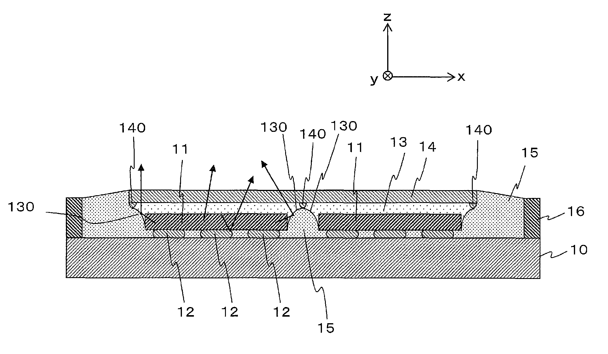
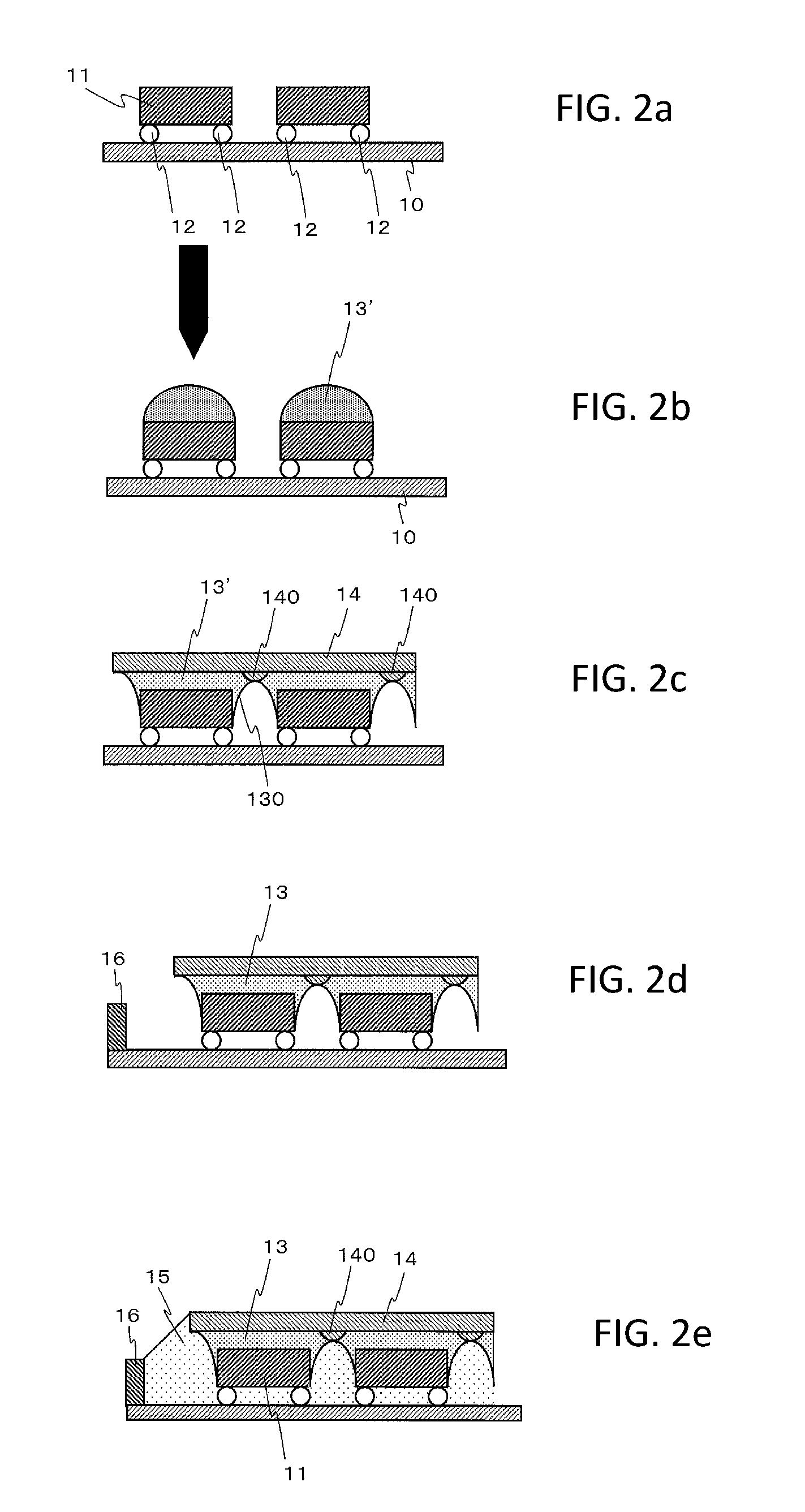
[0049]Exemplary embodiments and manufacturing methods of the disclosed subject matter will now be described in detail with reference to FIGS. 1 to 10b. FIG. 1 is a side cross-sectional view showing an exemplary embodiment of a semiconductor light-emitting device made in accordance with principles of the disclosed subject matter.

[0050]The semiconductor light-emitting device can include a base board 10 having a mounting surface and a conductor pattern (not shown in FIG. 1) formed on the mounting surface, and a plurality of semiconductor light-emitting chips 11 each having a top surface, a bottom surface, opposite side surfaces, second side surfaces located between the opposite side surfaces. Chip electrodes located adjacent the bottom surface of the light emitting chips 11 can be mounted on the mounting surface of the base board 10 via solder bumps 12. Each of the chip electrodes can be electrically connected to a respective portion of the conductor pattern of the base board 10 via th...


PUM


Abstract

A semiconductor light-emitting device and a method for manufacturing the same can include a wavelength converting layer in order to emit various colored lights including white light. The semiconductor light-emitting device can include a base board, a frame located on the base board, at least one light-emitting chip mounted on the base board, the wavelength converting layer located between an optical plate and each outside surface of the chips so as to extend toward the optical plate using a meniscus control structure, and a reflective material layer disposed at least between the frame and both side surfaces of the wavelength converting layer and the optical plate. The semiconductor light-emitting device can be configured to improve light-emitting efficiency and color variability between the light-emitting chips by using the reflective material layer as each reflector, and therefore can emit a wavelength-converted light having a high light-emitting efficiency from various small light-emitting surfaces.

Description

[0001]This application is a continuation-in-part application claiming priority under 35 U.S.C. §120 to co-pending U.S. patent application Ser. No. 13 / 162,151 filed on Jun. 16, 2011 entitled Semiconductor Light-Emitting Device And Manufacturing Method, which claims priority under 35 U.S.C. §119 of Japanese Patent Application No. 2010-137365 filed on Jun. 16, 2010. This application separately claims priority under 35 U.S.C. §119 of Japanese Patent Application No. 2010-276875 filed on Dec. 13, 2010. All of the above-referenced priority documents are hereby incorporated in their entirety by reference.BACKGROUND[0002]1. Field[0003]The presently disclosed subject matter relates to semiconductor light-emitting devices in which light emitted from at least one semiconductor light-emitting chip is wavelength-converted by a wavelength converting layer, and to manufacturing methods for the same. More particularly, the disclosed subject matter relates to semiconductor light-emitting devices for ...

Claims


Application Information

Patent Timeline
Patent Type & Authority Patents(United States)
IPC IPC(8): H01L29/20H01L33/00
CPCH01L25/0753H01L33/58H01L33/46H01L33/50H01L33/641H01L2924/09701H01L2224/48091H01L2224/48247H01L2224/73253H01L2924/00
Inventor WARAGAWA, TAKESHIITO, KOSABURO
Owner STANLEY ELECTRIC CO LTD
Why Eureka
Try Eureka