Semiconductor device and method for manufacturing same

a semiconductor and semiconductor technology, applied in the direction of semiconductor devices, basic electric elements, electrical appliances, etc., can solve the problems of deteriorating switching characteristics, increasing the recovery time, and affecting the recombination rate of minority carriers accumulated in the gap region, so as to reduce the recovery time and enhance the recombination rate of minority carriers

Inactive Publication Date: 2013-06-11
RENESAS ELECTRONICS CORP
View PDF7 Cites 0 Cited by
  • Summary
  • Abstract
  • Description
  • Claims
  • Application Information

AI Technical Summary

Benefits of technology

[0013]In such method for manufacturing the semiconductor device, the opening is formed above the gap region, which is a region between said first impurity-diffusing layer and said second impurity-diffusing layer, in addition to being formed in the portion above the first impurity-diffusing layer. Since this allows forming a damaged layer due to an injection of an impurity into the gap region, a recombination rate of minority carrier accumulated there can be enhanced.
[0015]In the semiconductor device, the electroconducting plug (second electroconducting plug) is provided above the gap region, in addition to being formed above the first impurity-diffusing layer. According to the semiconductor device having such configuration, an impurity is injected through the opening for the second electroconducting plug (second opening) during the manufacture thereof, such that a damaged layer is also formed in the above-described gap region. Actually, in the semiconductor device, an impurity is injected under the second opening portion Consequently, a recombination rate of minority carrier accumulated in the gap region can be enhanced.
[0016]According to the present invention, the semiconductor device having the structure suitable for reducing the recovering time and the method for manufacturing thereof are achieved.

Problems solved by technology

Consequently, a defective situation may be arisen in the operation due to an unexpected reverse current in some circuit.
Further, in bipolar transistors utilizing action of minority carrier, a problem of deteriorating the switching characteristic is also occurred by an increase of a recovering time.
While the recovery time can be ignored by employing the Schottky diode due to smaller amount of accumulated minority carrier, the use of the Schottky diode may cause problems of larger leakage current and difficulty in providing higher voltage-resistance.
However, when such solution is applied to integrated circuits, a problem of occurring non-negligible influences to other devices is caused.

Method used


Image

  • Semiconductor device and method for manufacturing same
  • Semiconductor device and method for manufacturing same
  • Semiconductor device and method for manufacturing same

Examples


first embodiment

[0032

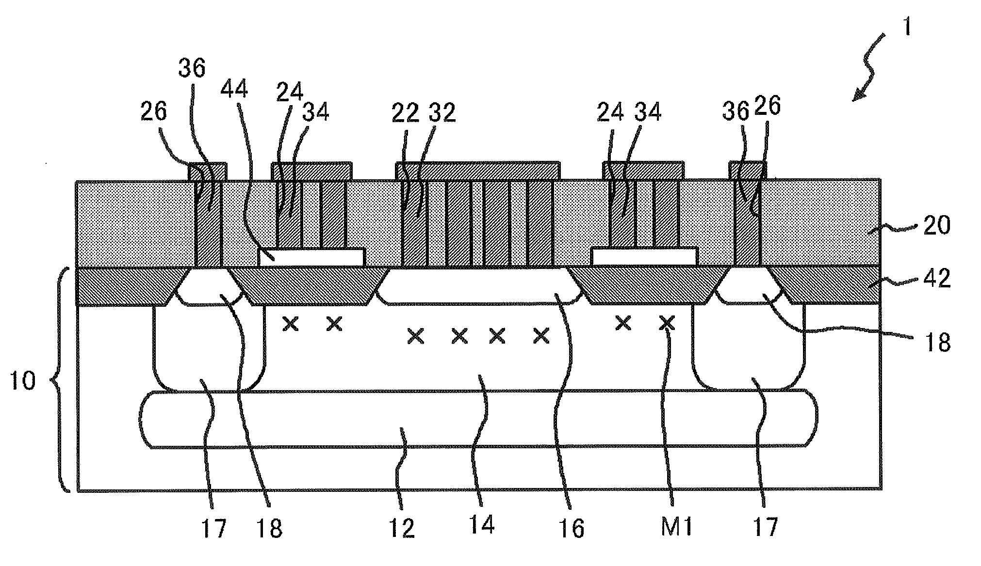
[0033]FIG. 1 is a cross-sectional view, illustrating first embodiment of a semiconductor device according to the present invention. A semiconductor device 1 includes a semiconductor substrate 10, a contact plug 32 (first electroconducting plug) and a contact plug 34 (second electroconducting plug). In the present embodiment, the semiconductor substrate 10 is a p-type silicon substrate. An n+ type buried region 12 is formed in the semiconductor substrate 10. An n-type region 14 is formed on the n+ type buried region 12, and a p-type diffusion layer 16 is formed in a surface layer of the n-type region 14. The n-type region 14 and the p-type diffusion layer 16 constitute a diode. Further, an n+ type region 17 extending from the surface of the semiconductor substrate 10 is formed so as to reach the n+ type buried region 12. An n-type diffusion layer 18 is formed in a surface layer of the n+ type region 17. Such n-type diffusion layer 18 functions as a contact layer of the n-type re...

second embodiment

[0050

[0051]FIG. 7 is a cross-sectional view, illustrating second embodiment of a semiconductor device according to the present invention. While first embodiment illustrates the exemplary implementation of applying the configuration of the present invention to the diode, the present embodiment is an exemplary implementation of applying the present invention to bipolar transistors. A semiconductor device 2 includes a p-type region 52 serving as a base of a bipolar transistor, formed in an n-type region 14 of a semiconductor substrate 10. The n-type region 14 functions as a collector of the bipolar transistor. A p+ type diffusion layer 54 (first impurity-diffusing layer) and an n+ type diffusion layer 56 (second impurity-diffusing layer) are formed in the surface layer of the p-type region 52. The p+ type diffusion layer 54 functions as a contact layer of the p-type region 52, and the n+ type diffusion layer 56 functions as an emitter of the above-described bipolar transistor.

[0052]An ...


PUM


Abstract

In conventional processes, a recombination rate of minority carrier accumulated between a diffusion layer of an anode and a diffusion layer of a cathode cannot be enhanced. An interlayer insulating film 20 is formed on a semiconductor substrate 10. An opening 22 (first opening), an opening 24 (second opening) and an opening 26 are formed in the interlayer insulating film 20. The opening 22 and the opening 26 are formed above respective the p-type diffusion layer 16 and the n-type diffusion layer 18. The opening 24 is formed above the gap region that is a region between the p-type diffusion layer 16 and the n-type diffusion layer 18. A contact plug 32, a contact plug 34 and a contact plug 36 are embedded in the opening 22, the opening 24 and the opening 26 respectively. Both regions of the semiconductor substrate 10 located under the opening 22 among and located under the opening 24 are doped with an impurity.

Description

[0001]This application is based on Japanese patent application No. 2006-206,051, the content of which is incorporated hereinto by reference.BACKGROUND[0002]1. Technical Field[0003]The present invention relates to a semiconductor device and a method for manufacturing thereof.[0004]2. Related Art[0005]It is known that a reverse current is flowed as shown in FIG. 11, when an operation of a PN junction diode is switched from a forward operation to an off state [see, for example, “Physics of Semiconductor Device”, authored by S. M. Sze, passages 2. 6. 1 (Transient Behavior), 2. 7. 5 (Fast-Recovery Diode), and 2. 7. 6 (Charge-Storage Diode)]. This is a phenomenon, which is occurred by reducing a concentration of a minority carrier, which has been accumulated in a diffusion layer in the forward operation of the diode, to an original concentration in a switch to an off state. The minority carrier is recombined in a diffusion layer to be dissipated, or, when an electric current path is prese...

Claims


Application Information

Patent Timeline
Patent Type & Authority Patents(United States)
IPC IPC(8): H01L29/861H01L21/20H01L21/331
CPCH01L21/26506H01L29/66272H01L29/7322H01L29/861
Inventor SATO, MASAHARU
Owner RENESAS ELECTRONICS CORP
Why Eureka
Try Eureka