Body contacted hybrid surface semiconductor-on-insulator devices
a hybrid surface semiconductor and on-insulator technology, applied in the field of body contact hybrid surface semiconductor on-insulator devices, can solve the problems that the floating body effect may limit the performance parameters of the hssoi device, and achieve the effect of minimizing or eliminating the floating body effect of the hssoi mos
- Summary
- Abstract
- Description
- Claims
- Application Information
AI Technical Summary
Benefits of technology
Problems solved by technology
Method used
Image
Examples
second embodiment
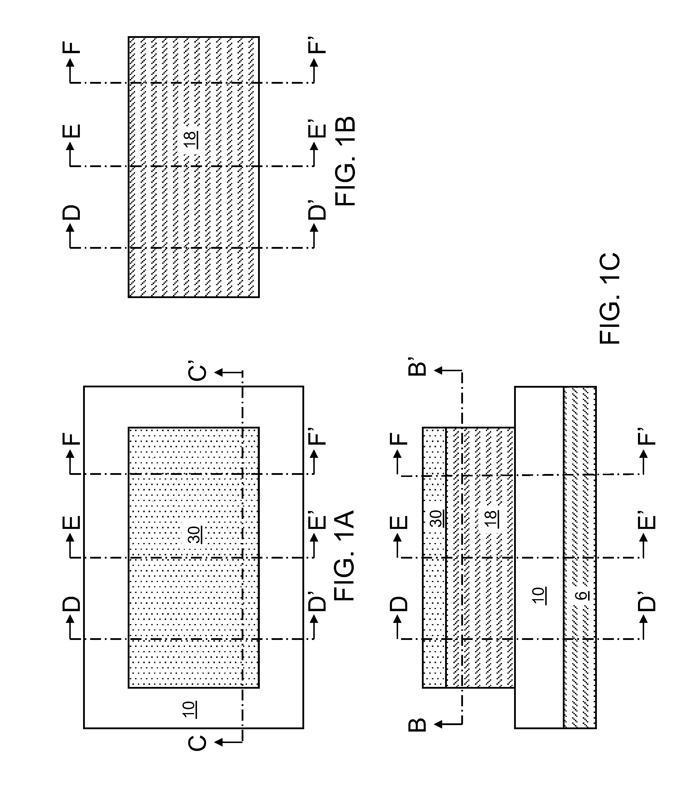
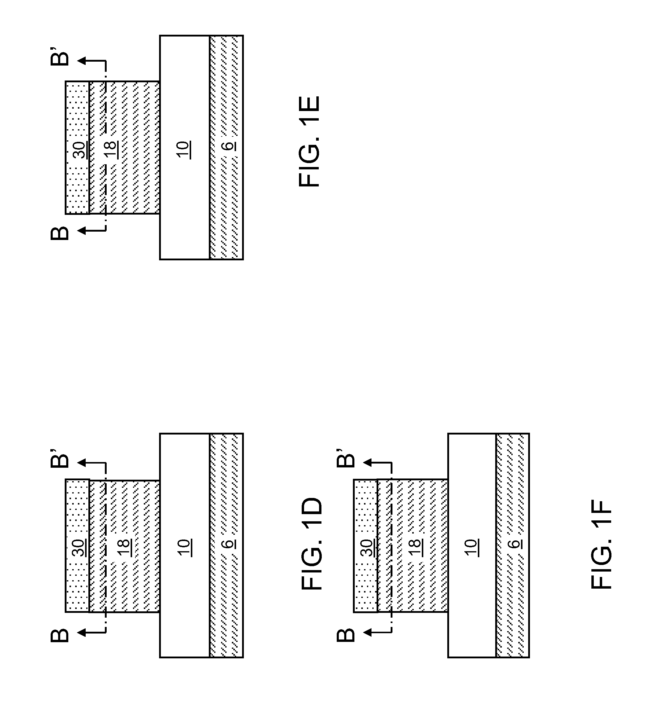
[0071]Referring to FIGS. 9A-9F, a second exemplary semiconductor structure according to the present invention is derived from the first exemplary semiconductor structure of FIGS. 2A-2F. A photoresist 57 is applied over the semiconductor fin 18 and the dielectric fin cap portion 30 and is lithographically patterned to mask the first end of the semiconductor fin 18, while exposing the second end of the semiconductor fin 18. An edge of the photoresist 57 may overlie the gate conductor 50. Alternately, an edge of the photoresist may overlie the gate spacer 55 and completely cover the gate conductor 50. A sub-portion of the dielectric fin cap portion 30 located above the second end of the semiconductor fin 18 is exposed. An anisotropic etch is employed to remove the sub-portion of the dielectric fin cap portion 30 that is not covered by the gate conductor 50 or the photoresist 57. In the case where an edge of the photoresist 57 overlies the gate conductor 50, the gate conductor 50 and th...
first embodiment
[0074]The implantation depth of the dopants of the second conductivity type is selected to be less than one half of the width of the semiconductor fin 18, and, more typically, to a location slightly away from the fin sidewalls. First and second source regions 62 are formed directly beneath the portion of the first sidewall at the first end and directly beneath the portion of the second sidewall at the first end in the same manner as in the
[0075]The drain region 66 extends from an edge of the first gate dielectric across the portion of the first sidewall on the second end to the second end wall, across the second end wall, across the second sidewall on the second end of the semiconductor fin 18, and to an edge of the second gate dielectric in the lateral direction. The drain region also extends from the first sidewall on the second end, up to the top surface of the second end of the semiconductor fin 18, across the top surface of the second end of the semiconductor fin 18, and to the...
fourth embodiment
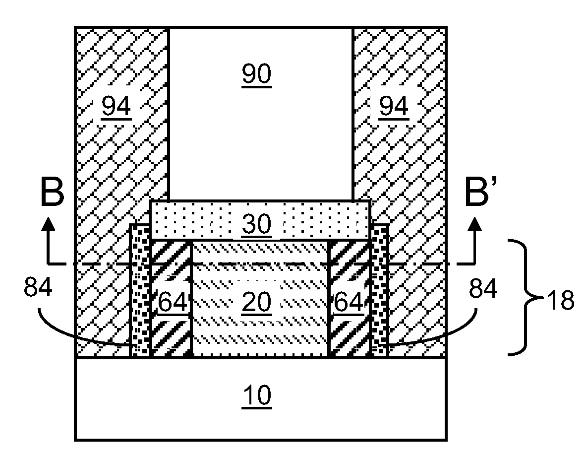
[0103]Referring to FIGS. 18A-18F, a fourth exemplary semiconductor structure according to the present invention is derived from the first exemplary semiconductor structure by omitting the formation of the modified semiconductor region 72 at the processing step corresponding to FIGS. 5A-5F. Thus, the source-side metal semiconductor alloy portion 82 abuts the first and second source regions 62 and the portion of the body region 20 located between the first and second source regions 62. As in the previous embodiments, the HSSOI MOSFET may be oriented to take advantage of crystallographic orientations that may be selected from all possible orientations of the first and second sidewalls. The body region 20 of the HSSOI MOSFET is electrically connected to the source-side metal semiconductor alloy portion 82 directly.
PUM
 Abstract
Description
Claims
Application Information


