Body contacted hybrid surface semiconductor-on-insulator devices

Active Publication Date: 2010-06-24
AURIGA INNOVATIONS INC
View PDF24 Cites 45 Cited by
  • Summary
  • Abstract
  • Description
  • Claims
  • Application Information

AI Technical Summary

Benefits of technology

[0004]An embodiment of the present invention provides a hybrid surface semiconductor-on-insulator (HSSOI) metal-oxide-semiconductor field effect

Problems solved by technology

Particularly, the floating body effect may place a l

Method used


Image

  • Body contacted hybrid surface semiconductor-on-insulator devices
  • Body contacted hybrid surface semiconductor-on-insulator devices
  • Body contacted hybrid surface semiconductor-on-insulator devices

Examples


second embodiment

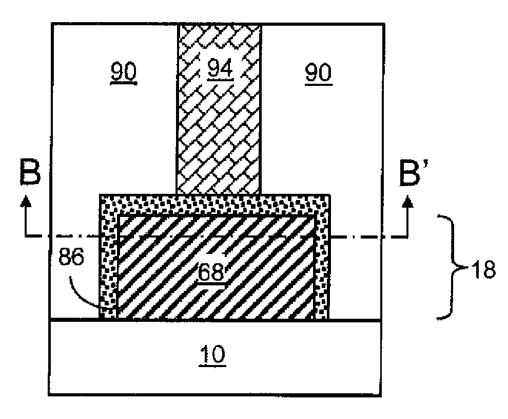
[0070]Referring to FIGS. 9A-9F, a second exemplary semiconductor structure according to the present invention is derived from the first exemplary semiconductor structure of FIGS. 2A-2F. A photoresist 57 is applied over the semiconductor fin 18 and the dielectric fin cap portion 30 and is lithographically patterned to mask the first end of the semiconductor fin 18, while exposing the second end of the semiconductor fin 18. An edge of the photoresist 57 may overlie the gate conductor 50. Alternately, an edge of the photoresist may overlie the gate spacer 55 and completely cover the gate conductor 50. A sub-portion of the dielectric fin cap portion 30 located above the second end of the semiconductor fin 18 is exposed. An anisotropic etch is employed to remove the sub-portion of the dielectric fin cap portion 30 that is not covered by the gate conductor 50 or the photoresist 57. In the case where an edge of the photoresist 57 overlies the gate conductor 50, the gate conductor 50 and th...

first embodiment

[0073]The implantation depth of the dopants of the second conductivity type is selected to be less than one half of the width of the semiconductor fin 18, and, more typically, to a location slightly away from the fin sidewalls. First and second source regions 62 are formed directly beneath the portion of the first sidewall at the first end and directly beneath the portion of the second sidewall at the first end in the same manner as in the

[0074]The drain region 66 extends from an edge of the first gate dielectric across the portion of the first sidewall on the second end to the second end wall, across the second end wall, across the second sidewall on the second end of the semiconductor fin 18, and to an edge of the second gate dielectric in the lateral direction. The drain region also extends from the first sidewall on the second end, up to the top surface of the second end of the semiconductor fin 18, across the top surface of the second end of the semiconductor fin 18, and to the...

fourth embodiment

[0102]Referring to FIGS. 18A-18F, a fourth exemplary semiconductor structure according to the present invention is derived from the first exemplary semiconductor structure by omitting the formation of the modified semiconductor region 72 at the processing step corresponding to FIGS. 5A-5F. Thus, the source-side metal semiconductor alloy portion 82 abuts the first and second source regions 62 and the portion of the body region 20 located between the first and second source regions 62. As in the previous embodiments, the HSSOI MOSFET may be oriented to take advantage of crystallographic orientations that may be selected from all possible orientations of the first and second sidewalls. The body region 20 of the HSSOI MOSFET is electrically connected to the source-side metal semiconductor alloy portion 82 directly.


PUM


Abstract

A portion of a top semiconductor layer of a semiconductor-on-insulator (SOI) substrate is patterned into a semiconductor fin having substantially vertical sidewalls. A portion of a body region of the semiconductor fin is exposed on a top surface of the semiconductor fin between two source regions having a doping of a conductivity type opposite to the body region of the semiconductor fin. A metal semiconductor alloy portion is formed directly on the two source regions and the top surface of the exposed body region between the two source regions. The doping concentration of the exposed top portion of the body region may be increased by ion implantation to provide a low-resistance contact to the body region, or a recombination region having a high-density of crystalline defects may be formed. A hybrid surface semiconductor-on-insulator (HSSOI) metal-oxide-semiconductor-field-effect-transistor (MOSFET) thus formed has a body region that is electrically tied to the source region.

Description

BACKGROUND[0001]The present invention relates to semiconductor devices, and particularly, to body contacted hybrid surface semiconductor-on-insulator (HSSOI) devices formed on a semiconductor-on-insulator (SOI) substrate and methods of manufacturing the same.[0002]Hybrid surface semiconductor-on-insulator (HSSOI) devices refer to semiconductor devices formed employing a sidewall of a top semiconductor layer of a semiconductor-on-insulator (SOI) substrate. HSSOI devices may be formed on the same SOI substrate as a planar semiconductor device employing a semiconductor surface that is parallel to a top surface of the top semiconductor layer.[0003]Electrical characteristics of the HSSOI devices display features of typical SOI devices. Particularly, the floating body effect may place a limitation on performance parameters of HSSOI devices. An important factor in optimizing the power and performance advantages of HSSOI devices is precise control of the voltage of the floating body.BRIEF S...

Claims


Application Information

Patent Timeline
IPC IPC(8): H01L29/786H01L21/84
CPCH01L29/66795H01L29/7841H01L29/785H01L29/7833
Inventor ANDERSON, BRENT A.NOWAK, EDWARD J.
Owner AURIGA INNOVATIONS INC
Why Eureka
Try Eureka