Method for manufacturing organic light-emitting diodes

a technology of organic light-emitting diodes and manufacturing methods, which is applied in the manufacture of electric discharge tubes/lamps, cold cathodes, and electromechanical systems, etc., can solve the problems of reducing the effective recombination rate of electrons and holes, and achieves the effect of improving the luminance efficiency of organic light-emitting diodes and high energy levels

Inactive Publication Date: 2005-05-12
NAT CHENG KUNG UNIV
View PDF10 Cites 1 Cited by
  • Summary
  • Abstract
  • Description
  • Claims
  • Application Information

AI Technical Summary

Benefits of technology

[0006] According to a conventional organic light-emitting diode, the amount unbalance is between positive carriers and negative carriers, so the luminance efficiency of the organic light-emitting diode is reduced due to the ineffective recombination rate of the positive carriers and the negative carriers.
[0007] Therefore, one objective of the present invention is to provide a method for manufacturing an organic light-emitting diode, by adding nitrogen gas (N2) when a hole transport layer is grown, so as to dope nitrogen molecules into the hole transport layer. The nitrogen molecules in the hole transport layer have a higher energy level, so the holes can be trapped in the hole transport layer, thereby increasing the recombination rate of electrons and holes, reducing the waste of holes, and enhancing luminance efficiency of the organic light-emitting diode.
[0008] Another objective of the present invention is to provide a method for manufacturing an organic light-emitting diode by using a hole transport layer formed by simultaneously evaporating the material of the hole transport layer and nitrogen gas to dope nitrogen molecules into the hole transport layer and form high energy level impurities. As a result, most holes are confined in the hole transport layer to decrease the amount of the holes transporting to the electron transport layer. Therefore, the potential of the hole transport layer can be increased to make a greater portion of voltage between two ends of the organic light-emitting diode be across the electron transport layer, and increase an injection electric field of electrons. The amount of electrons and the amount of holes are more balanced to enhance luminance efficiency of the organic light-emitting diode.
[0011] A reaction gas, that can form impurities of high energy level in the hole transport layer, can be added and be simultaneously evaporated with the material of the hole transport layer, and holes are caught by the impurities of high energy level during the transport process of the holes and trapped in the hole transport layer, so that the effective recombination rate of the electrons and the holes can be effectively enhanced. Therefore, the objective of improving luminance efficiency of the organic light-emitting diode can be achieved with low process cost.

Problems solved by technology

According to a conventional organic light-emitting diode, the amount unbalance is between positive carriers and negative carriers, so the luminance efficiency of the organic light-emitting diode is reduced due to the ineffective recombination rate of the positive carriers and the negative carriers.

Method used


Image

  • Method for manufacturing organic light-emitting diodes
  • Method for manufacturing organic light-emitting diodes
  • Method for manufacturing organic light-emitting diodes

Examples


Embodiment Construction

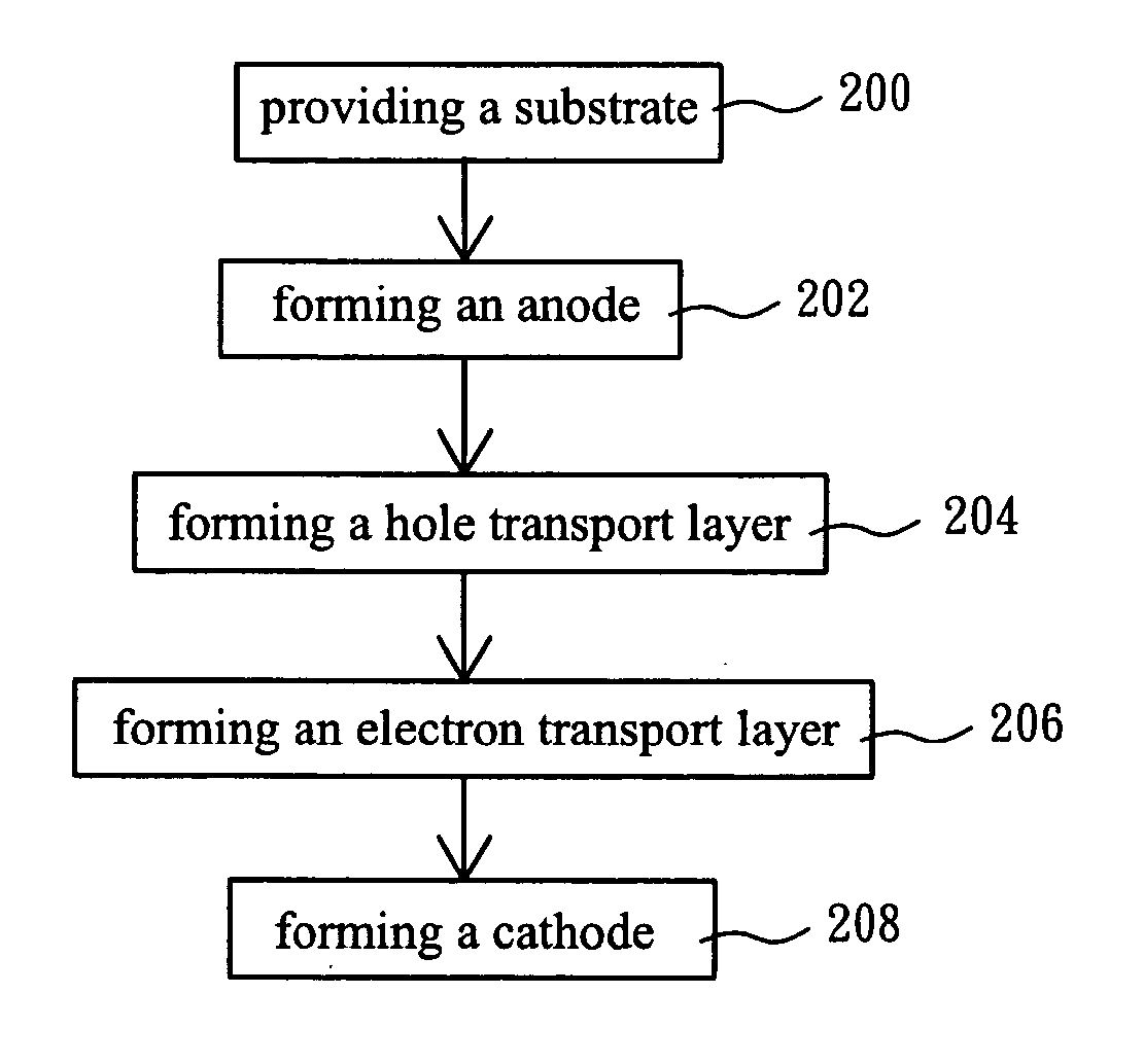
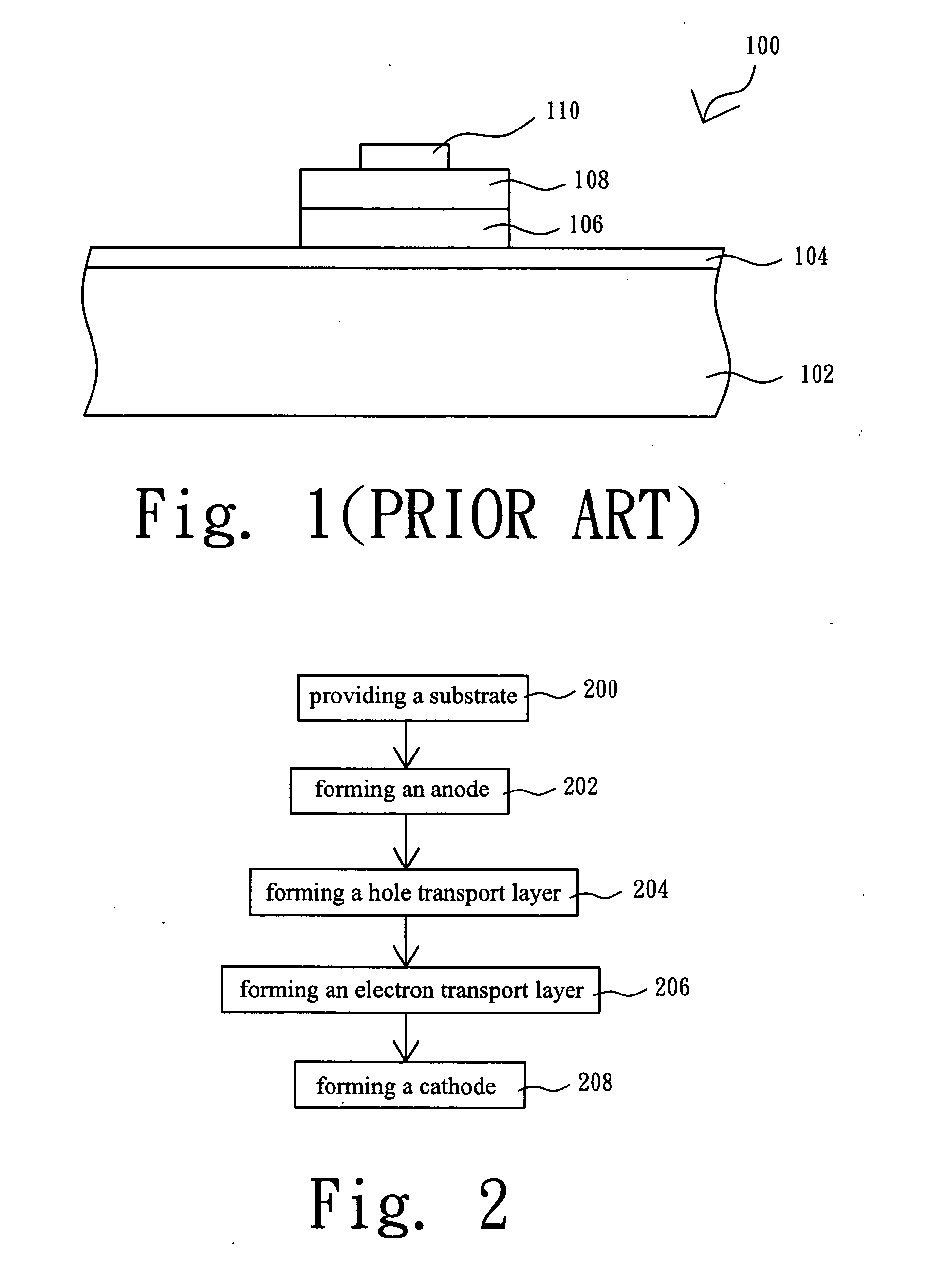
[0020] The present invention discloses a method for manufacturing an organic light-emitting diode, by adding a reaction gas that can form impurities with high energy level in a hole transport layer when growing the hole transport layer. These impurities with high energy level can confine holes in the hole transport layer, so as to increase effective recombination rate of electrons and holes injected into the electron transport layer, thereby achieving an objective of enhancing luminance efficiency with increasing process cost load. In order to make the illustration of the present invention more explicitly and completely, the following description and the drawings from FIG. 2 to FIG. 6 are stated.

[0021] Referring to FIG. 2, FIG. 2 illustrates a flowchart showing a process for manufacturing an organic light-emitting diode in accordance with a preferred embodiment of the present invention. First, in step 200, a transparent substrate is provided into a chamber, wherein the material of ...


PUM


Abstract

A method for manufacturing organic light-emitting diodes (OLEDs) is disclosed, by adding nitrogen (N2) into the material of a hole transport layer (HTL) and evaporating the nitrogen and the material of the hole transport layer while growing the hole transport layer, so as to dope nitrogen molecules into the hole transport layer. In the hole transport layer, the nitrogen molecules are impurities of higher energy level, and are used to catch holes while the holes transports and trap the holes in the hole transport layer, thereby obtaining an object of improving the luminance efficiency of the organic light-emitting diodes with lower cost.

Description

FIELD OF THE INVENTION [0001] The present invention relates to a method for manufacturing organic light-emitting diodes (OLEDs), and more particularly, to a process of organic light-emitting diodes that can effectively enhance the luminance current efficiency and the luminous Flux Power Efficiency. BACKGROUND OF THE INVENTION [0002] Referring to FIG. 1, FIG. 1 illustrates a cross-sectional view of a conventional organic light-emitting diode. A conventional organic light-emitting diode 100 includes a transparent substrate 102. An anode 104 is formed on the substrate 102, and a hole transport layer (HTL) 106 and an electron transport layer (ETL) 108 are formed to stack on the anode 104 in sequence. A cathode 110 is then formed on the electron transport layer 108. A carrier transport layer composed of the hole transport layer 106 and the electron transport layer 108 is located between the anode 104 and the cathode 110 for transporting holes and electrons. The electron transport layer 1...

Claims


Application Information

Patent Timeline
Patent Type & Authority Applications(United States)
IPC IPC(8): H01J9/00H05B33/10H01L51/00H01L51/40H01L51/50H01L51/56H05B33/14H05B33/22H05B33/26
CPCH01L51/0002H01L51/002H01L51/0059H01L2251/308H01L51/5048H01L51/56H01L51/0081H10K71/10H10K71/30H10K85/631H10K85/324H10K50/14H10K2102/103H10K71/00
Inventor FANG, YEAN-KUENLEE, WILLIAMHO, JYH-JIERTING, SHYH-FANNCHEN, SHIH-FANGCHIANG, HSIN-CHE
Owner NAT CHENG KUNG UNIV
Why Eureka
Try Eureka