Die singulation method

Active Publication Date: 2013-06-11
NAT TECH & ENG SOLUTIONS OF SANDIA LLC
View PDF9 Cites 2 Cited by
  • Summary
  • Abstract
  • Description
  • Claims
  • Application Information

AI Technical Summary

Benefits of technology

[0016]In some embodiments of the present invention wherein the die to be singulated include one or more MEMS devices, one of the steps of etching the first trench and etching the second trench can comprise etching moveable features of each MEMS device located on the die being singulated. In these embodiments, the step of etching away the oxide layer between the first trench and the second trench can also be used to etch away the oxide layer from beneath the moveable features of the MEMS device, thereby releasing the MEMS device. An offset dist

Problems solved by technology

The use of saw cutting requires a spacing (i.e. a street) between adjacent devices which are being singulated with this spacing being up to 100 microns or more wide; and this spacing limits the number of devices which can be fabricated from the semiconductor wafer.
Additionally, saw cutting generates debris which can contaminate the devices or become lodged in moveable members of MEMS devices or in fluid channel

Method used


Image

  • Die singulation method
  • Die singulation method
  • Die singulation method

Examples


Embodiment Construction

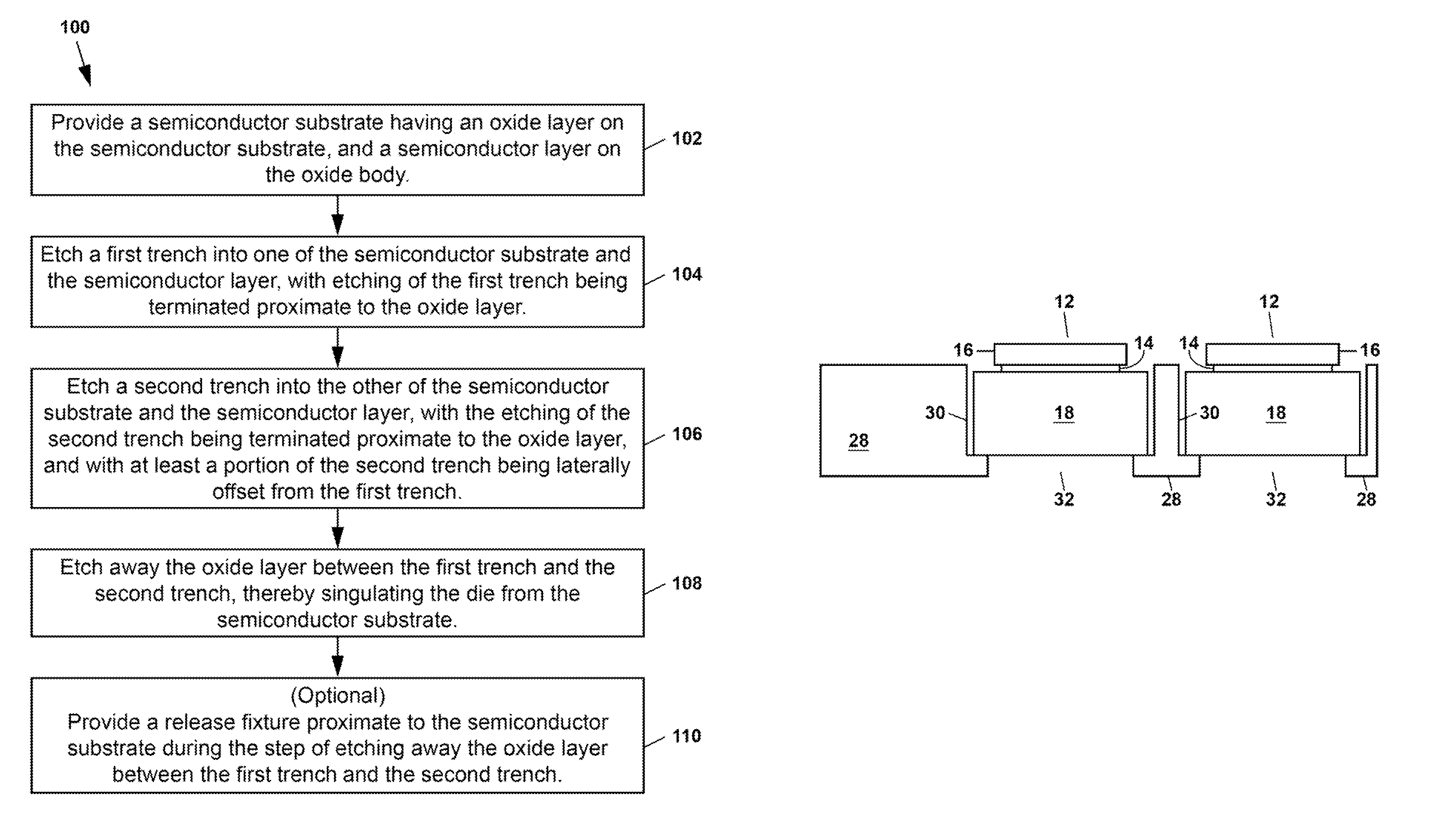
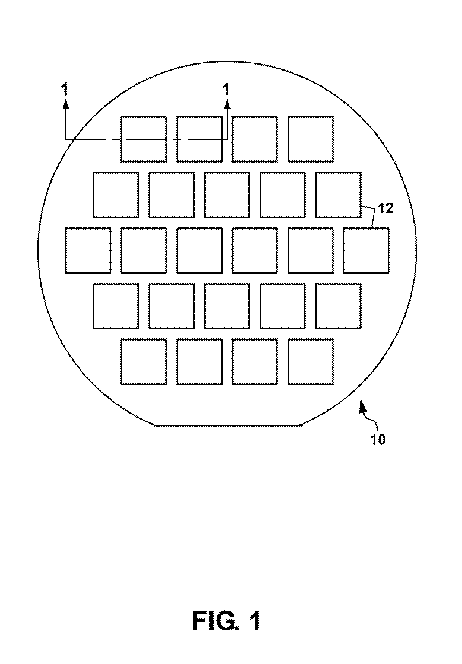
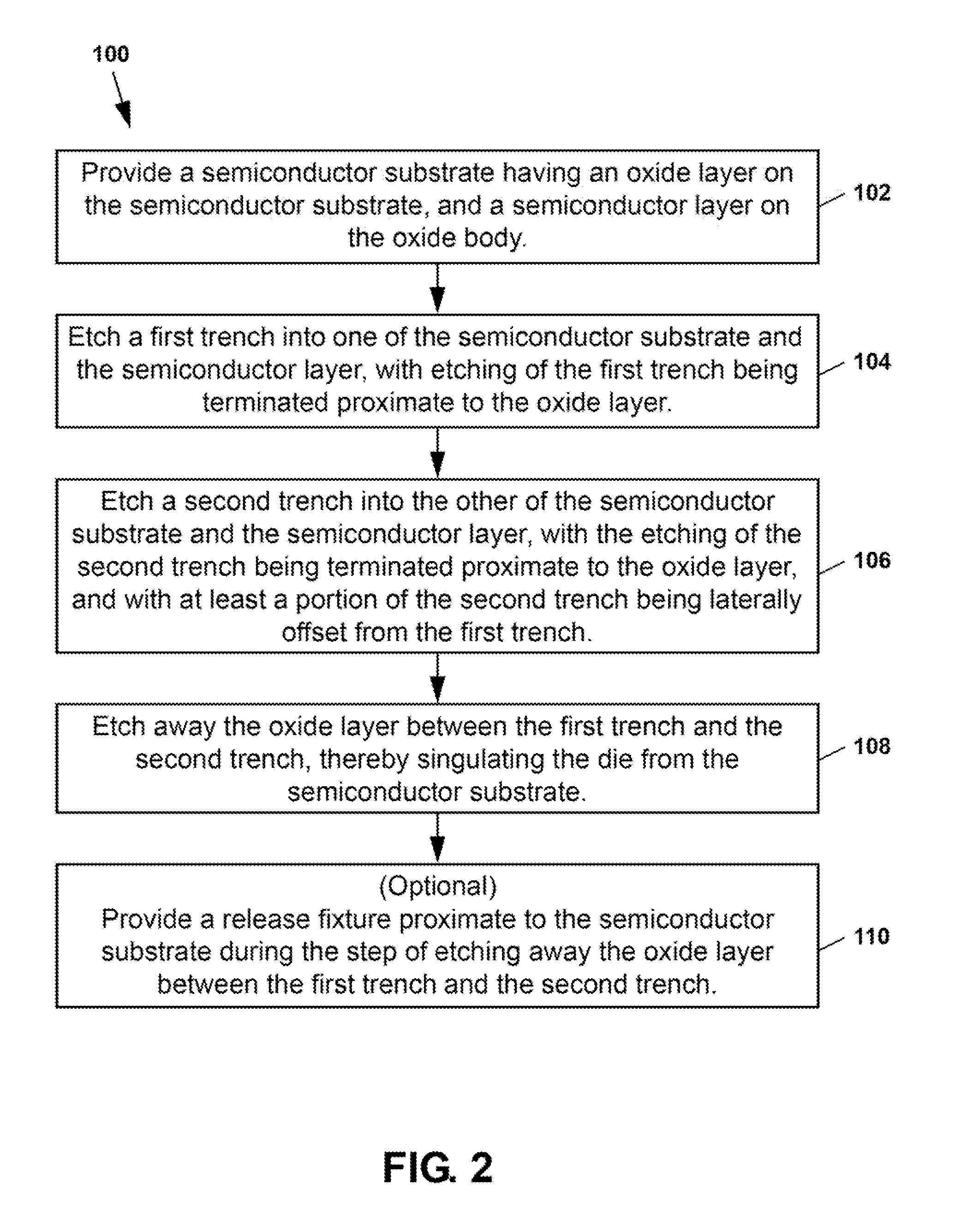
[0035]FIG. 1 shows a schematic plan view of a semiconductor substrate 10 having a plurality of die 12 formed thereon prior to singulation of the die 12 according to the method 100 of the present invention. Various steps in the method 100 for singulating the die 12 from the semiconductor substrate 10 are illustrated in FIG. 2 and will be described hereinafter with reference to FIGS. 3A-3E which show a series of schematic partial cross-section views along the section line 1-1 in FIG. 1.

[0036]The term “die” as used herein, which can be either singular or plural, refers to a portion of the substrate 10 wherein at least one semiconductor device such as an integrated circuit (IC), a microelectromechanical system (MEMS) device, a microfluidic device, a sensor, or a combination thereof is formed by a series of well-known semiconductor processing steps. The terms “singulation” and “singulating” as used herein refer to separating one or more of the die 12 from the semiconductor substrate 10 w...


PUM


Abstract

A method is disclosed for singulating die from a semiconductor substrate (e.g. a semiconductor-on-insulator substrate or a bulk silicon substrate) containing an oxide layer (e.g. silicon dioxide or a silicate glass) and one or more semiconductor layers (e.g. monocrystalline or polycrystalline silicon) located above the oxide layer. The method etches trenches through the substrate and through each semiconductor layer about the die being singulated, with the trenches being offset from each other around at least a part of the die so that the oxide layer between the trenches holds the substrate and die together. The trenches can be anisotropically etched using a Deep Reactive Ion Etching (DRIE) process. After the trenches are etched, the oxide layer between the trenches can be etched away with an HF etchant to singulate the die. A release fixture can be located near one side of the substrate to receive the singulated die.

Description

GOVERNMENT RIGHTS[0001]This invention was made with Government support under Contract No. DE-AC04-94AL85000 awarded by the U.S. Department of Energy. The Government has certain rights in the invention.CROSS REFERENCE TO RELATED APPLICATIONS[0002]The present application is related to a U.S. patent application entitled “Die Singulation Method and Package Formed Thereby” of common assignee which has Ser. No. 12 / 758,833 and which is being filed on the same date as this application, the contents of which are incorporated herein by reference in their entirety.FIELD OF THE INVENTION[0003]The present invention relates in general to semiconductor processing, and in particular to a method for singulating die from a semiconductor substrate by etching.BACKGROUND OF THE INVENTION[0004]A large number of semiconductor devices are typically fabricated on a common semiconductor wafer having a diameter up to 12 inches or more and then are separated (i.e. singulated) for packaging as individual device...

Claims


Application Information

Patent Timeline
IPC IPC(8): H01L21/301H01L21/48H01L21/78
CPCH01L21/78B81C1/00904H01L21/30655H01L21/31111
Inventor SWILER, THOMAS P.GARCIA, ERNEST J.FRANCIS, KATHRYN M.
Owner NAT TECH & ENG SOLUTIONS OF SANDIA LLC
Why Eureka
Try Eureka