Optical phase modulator

a phase modulator and optical phase technology, applied in the field of optical phase modulators and tunable interferometers, can solve the problems of limiting the application area of optical modulators, affecting the performance of optical waveguide light guides, and affecting the performance of optical waveguides, so as to reduce thermal drift of the overall electro-optical coefficient and reduce the optical phase drift

Inactive Publication Date: 2013-06-11
LUMENTUM OPERATIONS LLC
View PDF6 Cites 12 Cited by
  • Summary
  • Abstract
  • Description
  • Claims
  • Application Information

AI Technical Summary

Benefits of technology

[0014]According to the invention, an optical phase drift of an optical phase modulator can be lessened by combining on a single substrate waveguides of two types. An electrode structure is provided to create an electrical field in the waveguides of both types. The waveguides have, in conjunction with the electrode structure, opposite drifts of the electro-optical responses when an electrical field is applied to the waveguides. A positive drift of a waveguide of one type is compensated by a negative drift of a waveguide of the other type. In one embodiment, an Annealed Proton Exchange (APE) waveguide stitched to a Ti diffusion waveguide is disposed between a common pair of electrodes. A ratio of lengths of these two waveguides may be adjusted to further reduce thermal drift of the overall electro-optical coefficient of the optical phase modulator. Electrode gap, as well as a percentage of applied voltage, can also be adjusted or varied as required.
[0015]In accordance with the invention there is provided an optical phase modulator for modulating phase of an optical signal propagating therein, the optical phase modulator comprising an electro-optical substrate and an optical waveguide formed thereon or therein for guiding the optical signal. The optical waveguide comprises first and second waveguide portions optically coupled in series at a first stitch point, wherein the first and second waveguide portions comprise first and second materials, respectively. The optical phase modulator further comprises an electrode structure formed on or in the electro-optical substrate for creating an electric field in the first and second waveguide portions for modulating the phase. The first and second waveguide portions are characterized, in conjunction with the electrode structure, by first and second time drifts of magnitudes of their respective electro-optical responses when the electrical field is applied by the electrode structure to the first and second waveguide portions. The first and second time drifts are of opposite sign, whereby the time drift of the first waveguide portion at least partially compensates the time drift of the second waveguide portion. As a result, a time drift of an overall electro-optical response of the optical phase modulator is lessened.
[0016]In one embodiment, the optical waveguide further comprises a third waveguide portion optically coupled in series with the first and the second waveguide portions at a second stitch point, wherein the third waveguide portion comprises a third material. The electrode structure is configured for creating an electric field in the third waveguide portion for modulating phase. The third waveguide portion is characterized, in conjunction with the electrode structure, by a time drift of a magnitude of its electro-optical response, of an opposite sign than the time drift of the magnitude of the electro-optical response of the first waveguide portion. The time drift of the electro-optical response of the first waveguide portion is characterized by first and second time constants. The time drifts of the electro-optical response of the second and third waveguide portions are characterized by third and fourth time constants, respectively, substantially equal in magnitude to the first and second time constants, respectively, of the time drift of the electro-optical response of the first waveguide portion. As a result, the time drift of the overall electro-optical response of the optical phase modulator is further lessened.
[0017]The electrode network can include a resistive and / or capacitive and / or reactive voltage divider for dividing a voltage of the source of the electrical signal according to a ratio of lengths of the first and second waveguide portions and / or electrode gap widths at the first and second waveguide portions, so as to further reduce the time drift of the overall electro-optical response of the optical phase modulator. Temperature variable components can be used for reducing thermal dependence of the overall electro-optical response of the optical phase modulator.
[0024]wherein the first and second time drifts are of opposite sign, whereby the time drift of the first waveguide portion at least partially compensates the time drift of the second waveguide portion, thereby lessening a time drift of an overall electro-optical response of the optical phase modulator.

Problems solved by technology

Another known drawback of optical modulators having APE waveguides formed in lithium niobate substrates is associated with drift of electro-optical response in vacuum, due to instability of APE waveguides in vacuum.
The time drift of optical phase delay generated by the APE and Ti diffusion waveguide-based modulators 10 and 30 and YBBM 28 and 38, respectively, is highly detrimental and limits areas of their applications.

Method used


Image

  • Optical phase modulator
  • Optical phase modulator
  • Optical phase modulator

Examples


Embodiment Construction

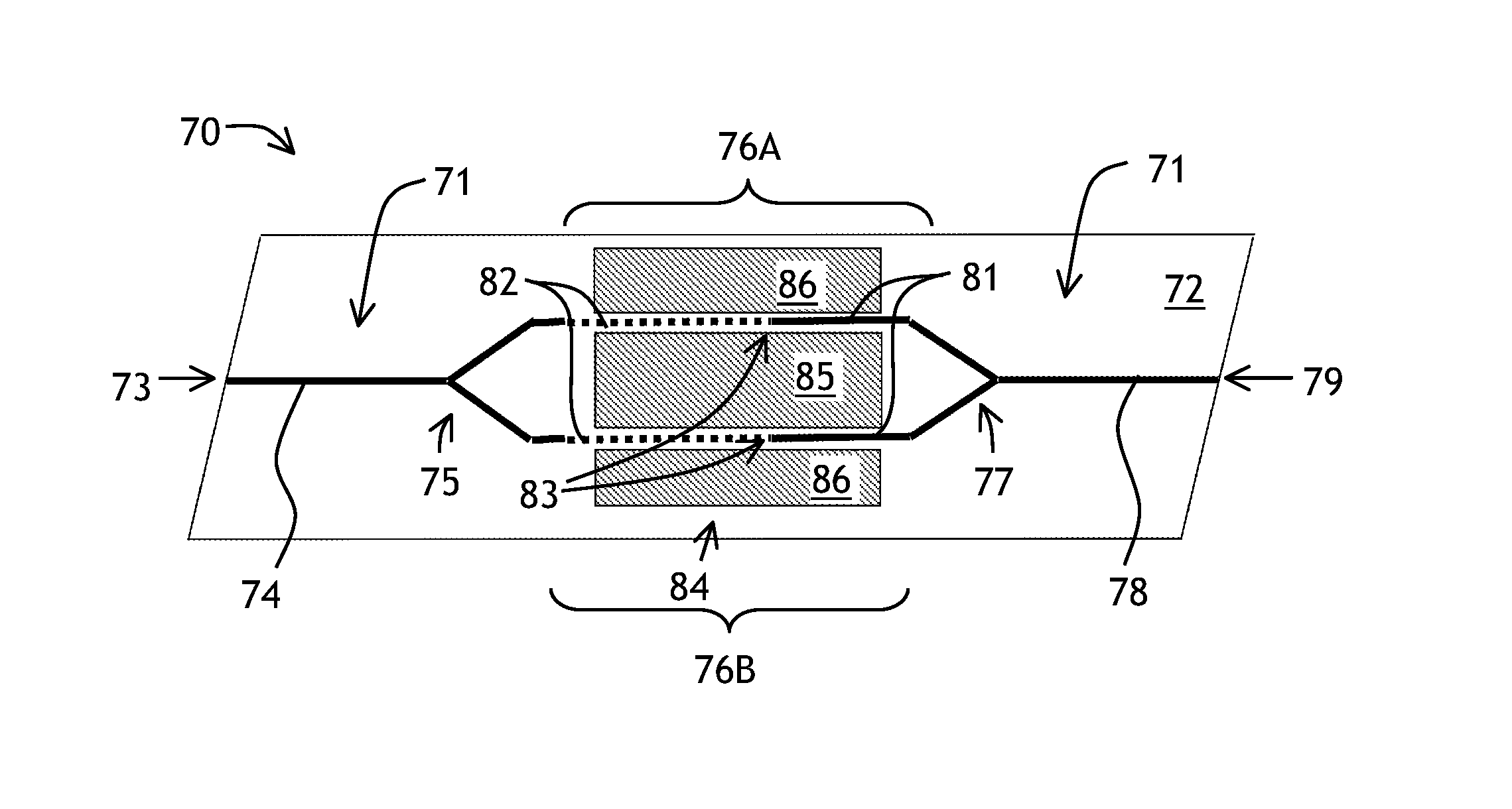
[0038]While the present teachings are described in conjunction with various embodiments and examples, it is not intended that the present teachings be limited to such embodiments. On the contrary, the present teachings encompass various alternatives, modifications and equivalents, as will be appreciated by those of skill in the art.

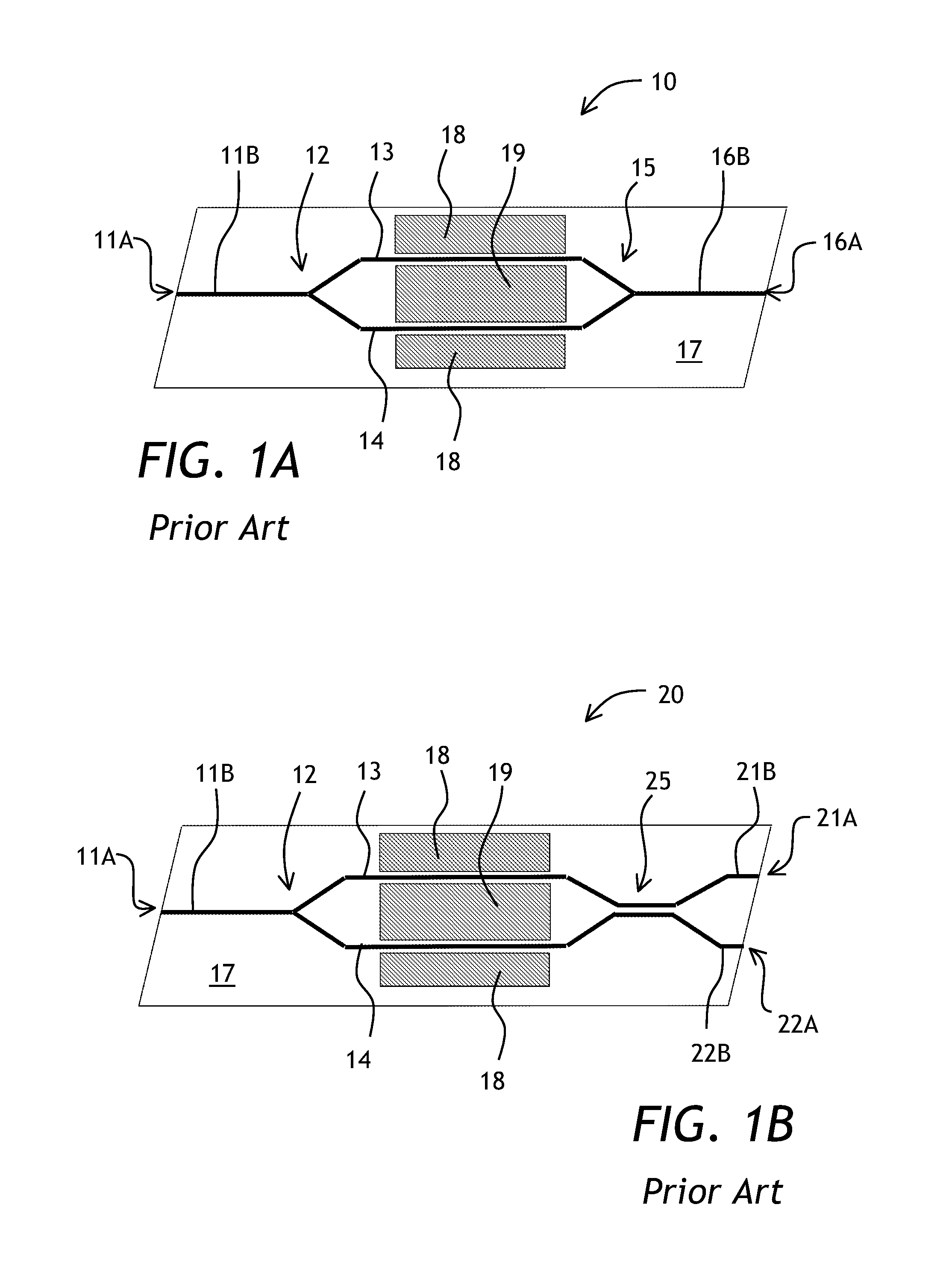
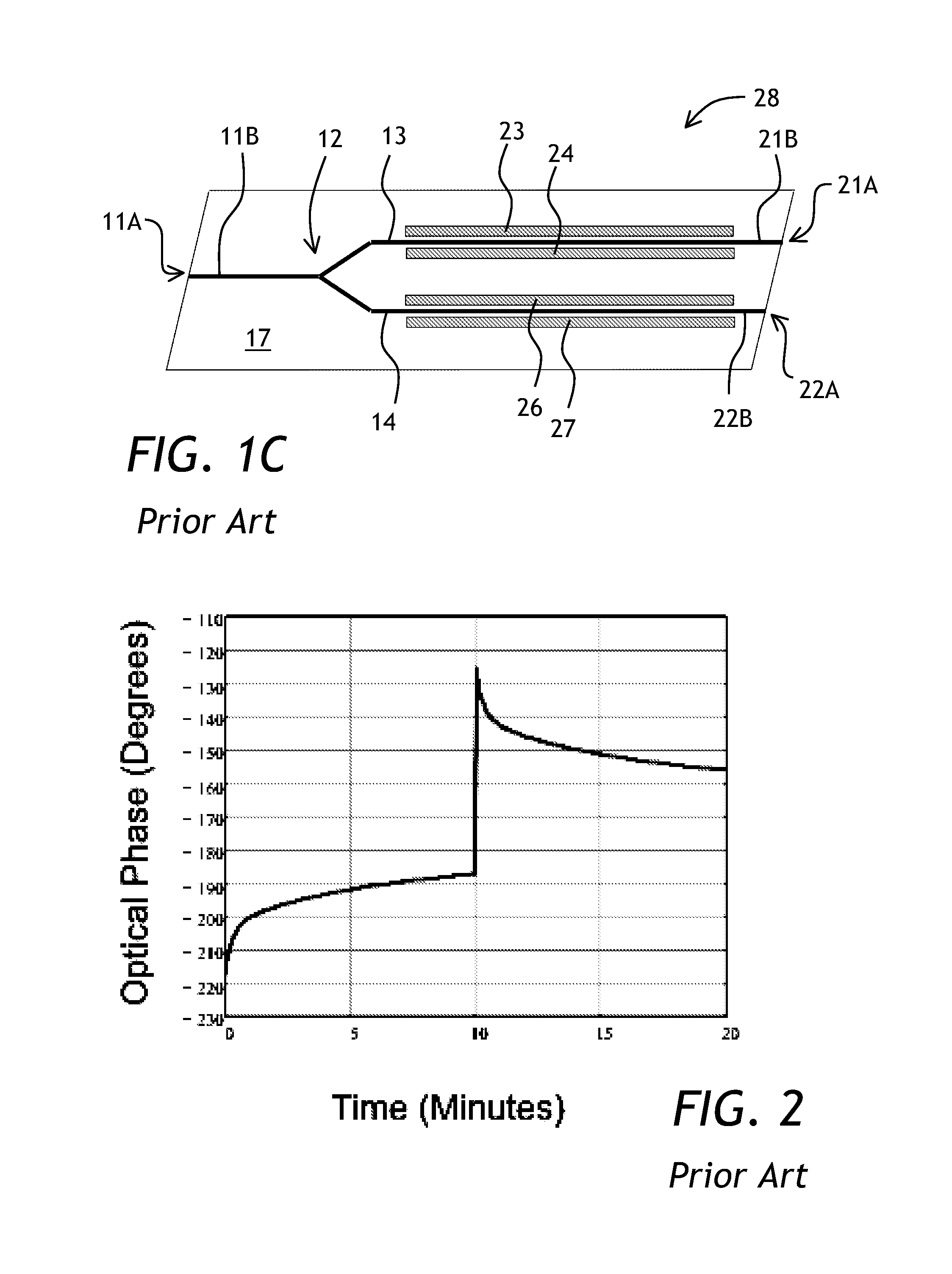
[0039]To better explain the invention and highlight advantages offered thereby, time drifts of electro-optical responses of prior-art APE- and Ti-diffusion waveguide optical phase modulators will be considered in more detail first.

[0040]The time drift of an electro-optical response of a prior-art APE waveguide optical phase modulator has been characterized by applying multiple voltage steps of different durations to the modulator's electrodes; measuring the resulting optical phase increments as a function of time; taking a Fourier transform of the optical phase measurements to obtain the optical phase as a function of frequency; and taking an inverse valu...


PUM

PropertyMeasurementUnit
temperaturesaaaaaaaaaa

Abstract

An optical phase modulator having a reduced time drift of an electro-optical response is disclosed. An optical waveguide exhibiting the electro-optic effect includes two serially coupled portions having opposite time drifts of magnitudes of their respective electro-optical responses. As a result, a time drift of an overall electro-optical response of the optical phase modulator is lessened.

Description

TECHNICAL FIELD[0001]The present invention relates to electro-optical devices, and in particular to optical phase modulators and tunable interferometers based thereon.BACKGROUND OF THE INVENTION[0002]Optical phase modulators are used to control phase of optical signals in interferometers and other devices where optical phase is translated into signal power, for example in Mach-Zehnder modulators used in optical communications and Sagnac interferometers used in optical gyroscopes. Functioning of most optical phase modulators is based on so-called electro-optic effect, wherein refractive index of an electro-optic material depends on an external electric field. The electric field is usually created by applying a voltage to a pair of electrodes disposed on two sides of the electro-optic material. Light propagating in the electro-optic material undergoes a phase shift due to a change of the refractive index caused in the material by the voltage applied to the electrodes. To lower the ope...

Claims


Application Information

Patent Timeline
Patent Type & Authority Patents(United States)
IPC IPC(8): G02F1/035G02F1/295G02F1/01G02F1/03G02B6/12G02B6/26
CPCG02F1/2255
Inventor KISSA, KARL
Owner LUMENTUM OPERATIONS LLC
Why Eureka
Try Eureka