Apparatus and method to remove at least one chip-like semiconductor component from a film

a technology of chip-like semiconductors and film, applied in the direction of electrical equipment, chemistry apparatus and processes, lamination ancillary operations, etc., can solve the problem of increasing the risk of damage, and achieve the effect of significantly reducing the risk of damage from removal

Inactive Publication Date: 2013-06-25
SEMIKRON ELECTRONICS GMBH & CO KG
View PDF11 Cites 7 Cited by
  • Summary
  • Abstract
  • Description
  • Claims
  • Application Information

AI Technical Summary

Benefits of technology

[0008]The object of the invention is to provide an improved apparatus and a method for removing at least one chip-type semiconductor component from a film, wherein the risk of damage from removal is significantly reduced.
[0013]Furthermore, it is advantageous if the lifting device includes a thermal device for changing the temperature of the adhesive film. Depending on the particular application, for example depending on the film used, in this case it can be expedient to vary, i.e., either decrease or increase the temperature of the film. A reduction of the temperature is appropriate, for example, in order to reduce the adhesive force between the film and the semiconductor component to be removed. An increase in the temperature is appropriate, for example, in order to increase the elasticity of the film.
[0018]The term “vacuum” designates the difference relative to atmospheric pressure (approximately 100 kPa), wherein larger values describe a larger difference and the suction effect is thus greater.
[0021]It can also be advantageous if the vacuum of one suction cutout or one group of suction cutouts is kept constant during the deformation, while the vacuum at another or a group of other suction cutouts is varied.
[0023]Finally, it is possible to remove the at least one semiconductor component from the film by means of the removal device.
[0024]Furthermore, it is advantageous to influence the temperature of the film during the lift-off process by means of a thermal device. In this case, the thermal element can increase the temperature of the film; alternatively or additionally, it can decrease the temperature thereof.

Problems solved by technology

The thinner the semiconductor component, the greater the risk of damage, in particular due to fracturing during removal thereof from the film.

Method used


Image

  • Apparatus and method to remove at least one chip-like semiconductor component from a film
  • Apparatus and method to remove at least one chip-like semiconductor component from a film
  • Apparatus and method to remove at least one chip-like semiconductor component from a film

Examples


second embodiment

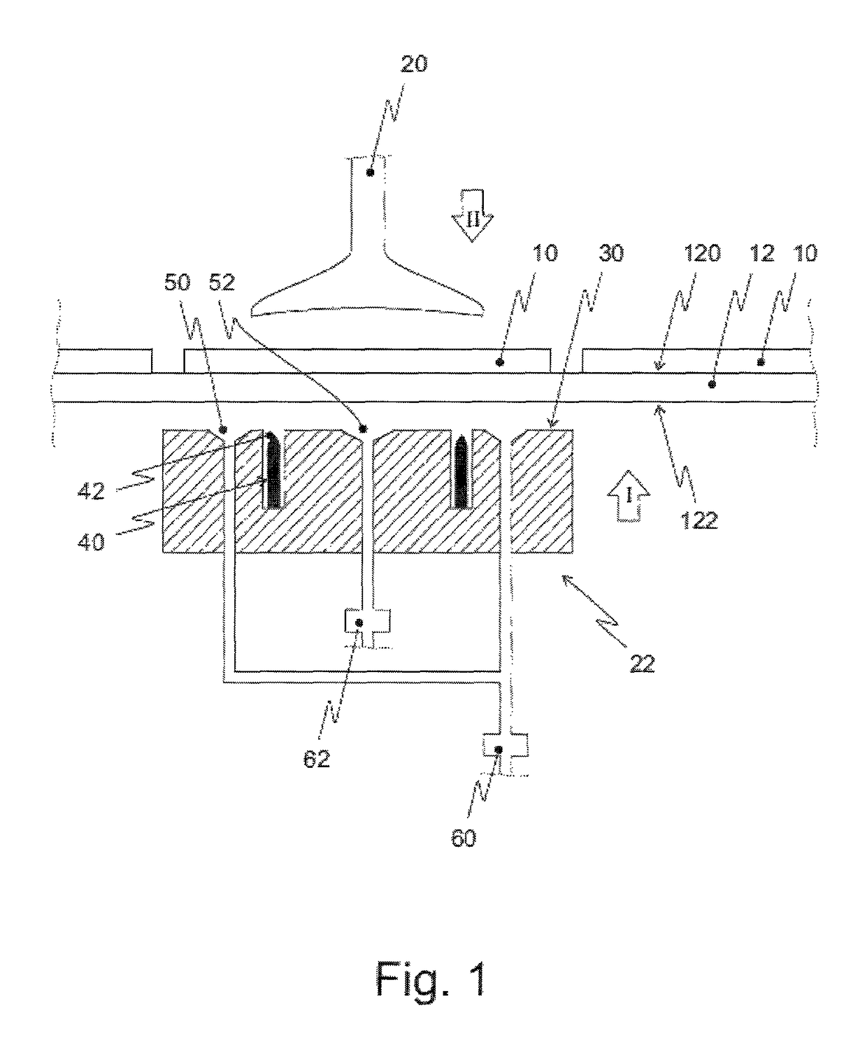
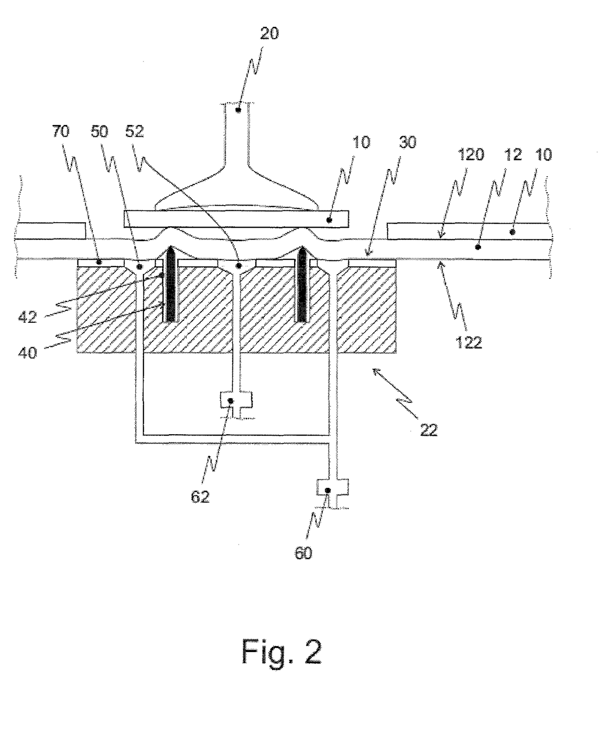
[0043]FIG. 2 shows a lateral section view of the inventive apparatus. The method step illustrated corresponds to that already described with respect to FIG. 1, wherein film 12 has already been deformed and semiconductor component 10 to be removed has already been lifted.

[0044]This embodiment of the inventive apparatus essentially differs from that shown in FIG. 1 by virtue of an additionally provided Peltier element 70, which here simultaneously, but not necessarily, forms contact region 30 of lifting device 22. In addition, the area of contact region 30 is made larger here and extends to below the adjacent semiconductor components 10.

[0045]Second vacuum regulating device 62 generates a constant vacuum of about 35 kPa at centrally arranged second suction cutouts 52, while first vacuum regulating device 60 applies a constant vacuum of about 40 kPa to the outer first suction devices 50. For the rest, the description given with respect to FIG. 1 applies to the choice and regulation of ...

third embodiment

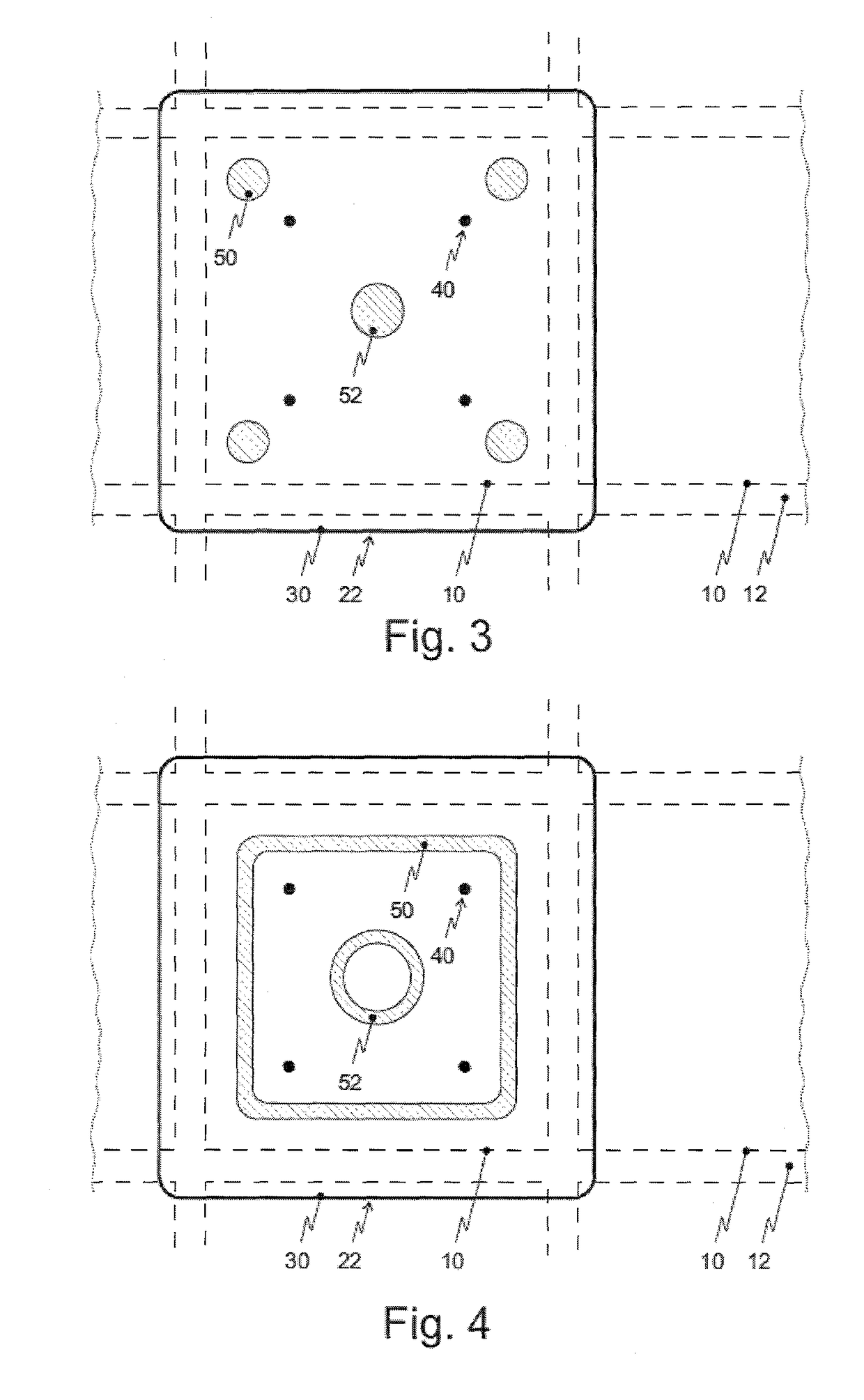
[0048]FIG. 4 schematically shows a plan view of the inventive apparatus. In contrast to the embodiment shown in FIG. 3, here only one first 50 and one second suction device 52 are provided, which are respectively connected to an assigned first and second vacuum regulating device (not illustrated).

[0049]In this case, both suction devices 50, 52 are embodied as trenches and not as circular holes, as illustrated in FIG. 3. The description given above is applicable with regard to the regulation of the vacuum applied thereto.


PUM

PropertyMeasurementUnit
temperatureaaaaaaaaaa
thicknessaaaaaaaaaa
thicknessaaaaaaaaaa

Abstract

Apparatus and a method for operating the apparatus to remove at least one chip-type semiconductor component from an adhesive film. The method comprises: arranging a lifting device with respect to the film, wherein a contact region of the lifting device bears against a second main surface of the film, opposite a chip-type semiconductor component that is arranged on a first main surface and is to be lifted off. Then, applying either a constant vacuum to a plurality of suction cutouts of the lifting device, by means of an assigned vacuum regulating device, or applying different values of the vacuum for different suction cutouts or groups of suction cutouts. Next, partially deforming the film in the contact region by using lifting means arranged in assigned cutouts of the lifting device to lift the film. Finally, using a removal device to remove the at least one semiconductor component from the film.

Description

BACKGROUND OF THE INVENTION[0001]1. Field of the Invention[0002]The invention relates to an apparatus and a method for simultaneously removing at least one chip-type semiconductor component, in particular a semiconductor component having a thickness of less than about 130 μm, or preferably of less than about 100 μm, from a film. Such semiconductor components are present for example after the division of wafers arranged on an adhesive film. Advantageously, the semiconductor components are power semiconductor components such as IGBTs or power diodes.[0003]2. Description of the Related Art[0004]Semiconductor chips are often manufactured in arrays of individual chips positioned on an adhesive film. After an array of chips is manufactured, for example on a wafer, the wafer is cut apart, so that each individual chip or group of chips, is a separate item, facilitating their further processing[0005]After manufacturing is complete, the chips have to be removed from the adhesive film to which...

Claims


Application Information

Patent Timeline
Patent Type & Authority Patents(United States)
IPC IPC(8): B32B38/10
CPCH01L21/67132H01L21/67144Y10T156/1179Y10T156/1944Y10T156/1132Y10T156/1983Y10T156/1906Y10T156/1105H01L21/0273H01L21/302H01L21/304H01L21/30621H01L21/30625H01L21/31116H01L21/4896H01L21/67098H01L21/677H01L21/67712H01L21/6836H01L21/76H01L21/78
Inventor STUDT, ARMIN
Owner SEMIKRON ELECTRONICS GMBH & CO KG
Why Eureka
Try Eureka