Semiconductor device having hierarchical bit line structure

a technology of hierarchical bit lines and semiconductor devices, which is applied in the direction of information storage, static storage, digital storage, etc., can solve the problems of difficult to achieve the reduction in the size of memory cells, the reduction of the sensing margin in the refresh operation, and the restriction of the size of the memory cells, so as to suppress the decrease in the sensing margin, increase the coupling capacitance, and suppress the effect of the coupling nois

Inactive Publication Date: 2013-06-25
LONGITUDE SEMICON S A R L
View PDF15 Cites 9 Cited by
  • Summary
  • Abstract
  • Description
  • Claims
  • Application Information

AI Technical Summary

Benefits of technology

[0017]The invention may be applied to a memory cell array having a single-ended bit line configuration, or to a memory cell array having an open bit line structure. Further, when the first and second global bit lines are arranged along the same line in a first direction and the third and fourth global bit lines are arranged along the same line in the first direction with a predetermined pitch relative to the first and second global bit lines, a sufficient effect of suppressing the coupling noise can be obtained. Furthermore, when performing the refresh operation for retaining data of the memory cells as the first to fourth operations, the effect of the invention becomes remarkable. The refresh operation may be an auto refresh mode or a self refresh mode. However, the first to fourth operations are not limited to the refresh operation and may be a read operation or a write operation, to which the invention can be also applied.
[0018]As described above, according to the present invention, in order to deal with the problem of an increase in coupling noise between the adjacent global bit lines due to an increase in coupling capacitance therebetween with the miniaturization of the memory cell array having the hierarchical bit line structure, it is possible to perform the operation being divided into two parts in the first and second periods, and in the operation for one global bit line, the other global bit line can be used as a shield. Therefore, it is possible to suppress a decrease in sensing margin due to the coupling noise between the adjacent global bit lines, and to reduce the capacitance of the global bit lines to substantially half by the first and second switches. Thus, large effects of an increase in sensing margin in the refresh operation and a reduction in consumption current can be obtained with decreasing the size of the memory cells.
[0019]Further, by employing the configuration of the invention, the global bit lines do not need to be configured with the folded bit line structure and to be twisted, and therefore it is possible to obtain effects of an increase in sensing margin and a reduction in consumption current without an increase in chip area. Further, when employing the single-ended memory cell array, the invention can be effectively applied to a configuration including shared type global sense amplifiers.

Problems solved by technology

However, in such a configuration, there arises a problem that the sensing margin in the refresh operation is reduced by influence of coupling noise between adjacent global bit lines in the hierarchical bit line structure.
Therefore, inevitably size of each memory cell cannot be set lower than twice the pitch of global bit lines, therefore a reduction in size of the memory cell is restricted.
In this manner, in the conventional memory cell array employing the hierarchical bit line structure, it is difficult to achieve the reduction in size of the memory cells, the reduction in consumption current in the refresh operation, and prevention of the reduction in sensing margin due to the coupling noise, at the same time.

Method used


Image

  • Semiconductor device having hierarchical bit line structure
  • Semiconductor device having hierarchical bit line structure
  • Semiconductor device having hierarchical bit line structure

Examples


first embodiment

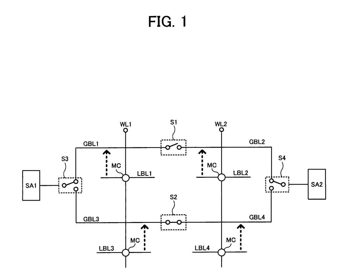
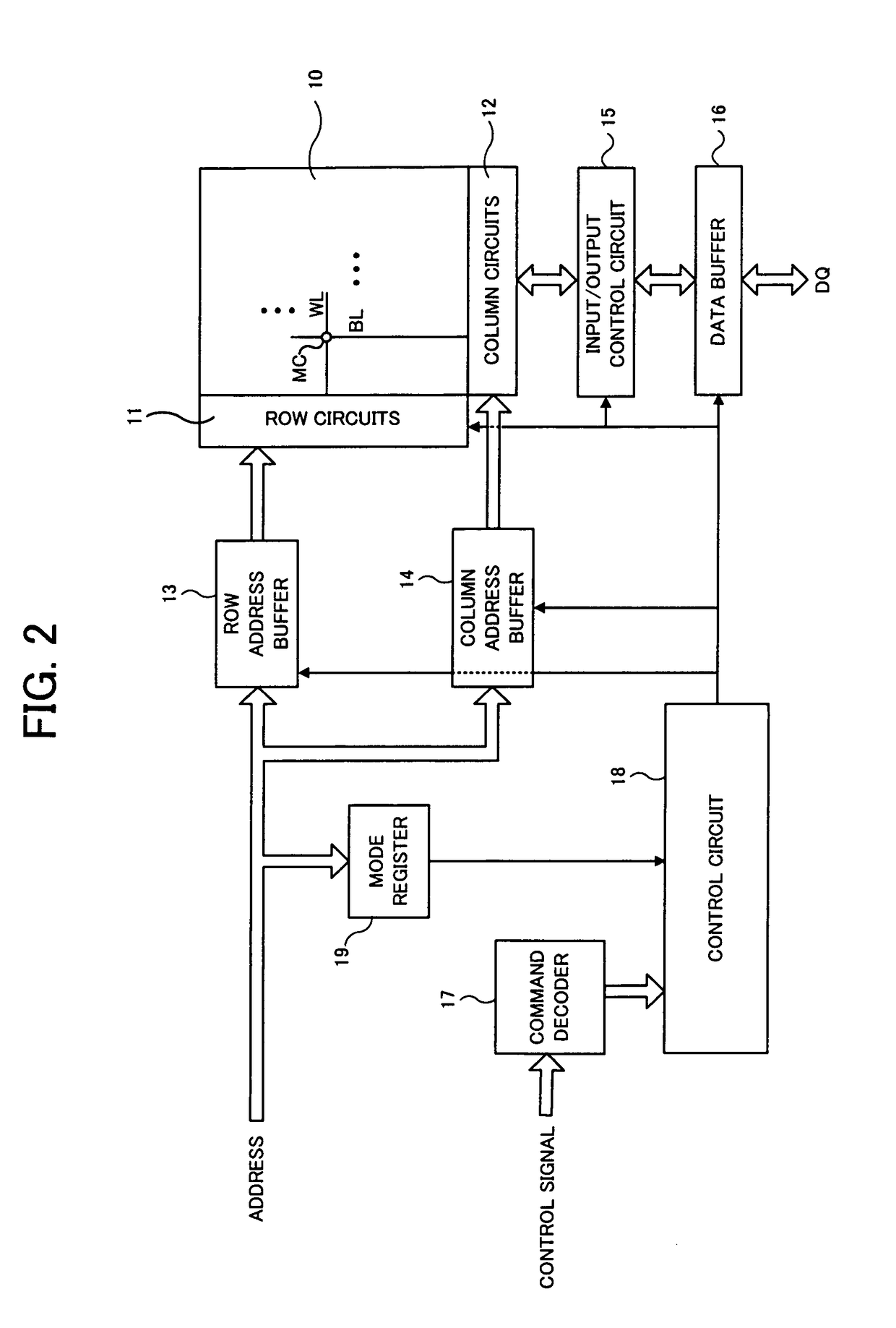
[0042]FIG. 2 is a block diagram showing an entire configuration of a DRAM of a first embodiment to which the invention is applied. The DRAM shown in FIG. 2 comprises a memory cell array 10 including a large number of memory cells MC arranged at intersections of a plurality of word lines WL and a plurality of bit lines BL (later describe local bit lines LBL), and row circuits 11 and column circuits 12 that are attached to the memory cell array 10. The row circuits 11 includes a large number of circuits provided corresponding to the plurality of word lines WL, and the column circuits 12 includes a large number of circuits provided corresponding to the plurality of bit lines BL. In addition, since the first embodiment employs a hierarchical bit line structure, the bit lines BL of the memory cell array 10 are hierarchized into global bit lines GBL of an upper hierarchy and local bit lines LBL of a lower hierarchy, which will be described in detail later.

[0043]Externally input addresses ...

second embodiment

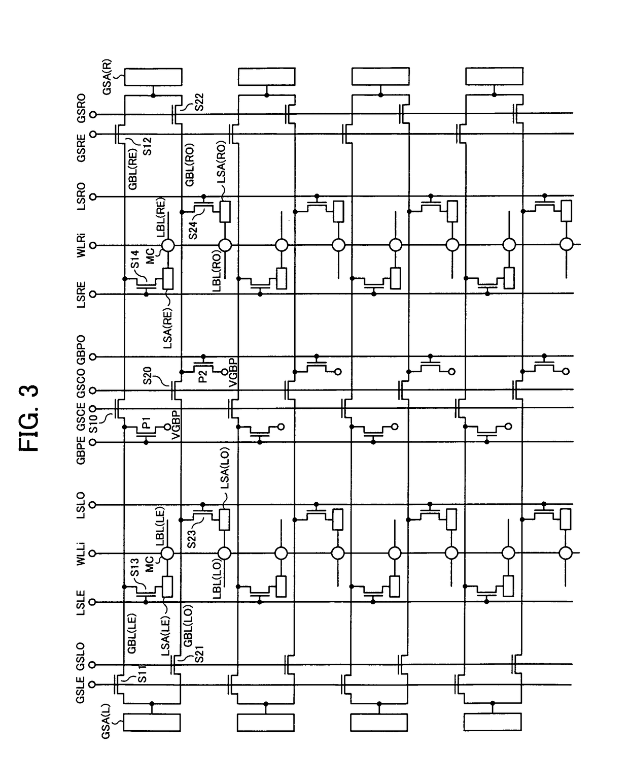
[0074]Next, a DRAM of a second embodiment to which the invention is applied will be described. The entire configuration of the DRAM of FIG. 2 is common in the second embodiment, so description thereof will be omitted. FIG. 13 is a diagram showing a configuration of the memory cell array 10 and its peripheral portion in the DRAM of the second embodiment, which shows a range corresponding to FIG. 3. As shown in FIG. 13, although the memory cell array 10 of the second embodiment employs the hierarchical bit line structure in the same manner as the first embodiment, it is different from the first embodiment that an open bit line structure is employed and sense amplifiers are not hierarchized in the second embodiment.

[0075]In FIG. 13, the arrangement of the global bit lines GBL and the local bit lines LBL, and the connection relations of the switches S10 to S12, S20 to S22 and the precharge transistors P1, P2 are the same as those in FIG. 3. Meanwhile, in FIG. 13, it is different from FI...


PUM


Abstract

A semiconductor device of the invention comprise a memory cell array configured with hierarchical local bit lines and global bit lines, in which there are provide local bit lines, global bit lines, switches controlling a connection between the global bit lines, sense amplifiers, and a control circuit controlling the switches. In a first period, each sense amplifier amplifies a signal of one of adjacent global bit lines, and in a second period, each sense amplifier amplifies a signal of the other thereof. Accordingly, coupling between the global bit lines can be suppressed.

Description

BACKGROUND OF THE INVENTION[0001]1. Field of the Invention[0002]The invention relates to a semiconductor device comprising a memory cell array in which a bit line structure is hierarchized using global bit lines and local bit lines.[0003]2. Description of Related Art[0004]In recent years, miniaturization of a memory cell array has been achieved in volatile semiconductor devices such as DRAM, and thus in order to overcome a performance problem caused by an increase in the number of memory cells connected to a bit line, a configuration in which the bit lines are hierarchized into global bit lines and local bit lines has been proposed. It is required to reduce memory cell size to, for example, 6F2 or 4F2 (“F” is minimum manufacturing scale), and a bit line pitch in this case needs to be set to 2F that is a manufacturing limit. Meanwhile, in a memory cell array having a hierarchical bit line structure, respective memory cells need to be refreshed in a refresh operation such as an auto r...

Claims


Application Information

Patent Timeline
Patent Type & Authority Patents(United States)
IPC IPC(8): G11C7/12G11C7/06
CPCG11C7/02G11C11/406G11C11/4094G11C11/4097
Inventor KAJIGAYA, KAZUHIKO
Owner LONGITUDE SEMICON S A R L
Why Eureka
Try Eureka