Transducer structure and method for MEMS devices

a transducer and transducer technology, applied in the field of integrated devices, can solve the problems of increasing complexity of microsystems that require greater computational power, and the limitations of ics, and in particular mems, and achieve the effect of convenient use and higher device yield

Active Publication Date: 2013-07-02
MCUBE INC
View PDF12 Cites 29 Cited by
  • Summary
  • Abstract
  • Description
  • Claims
  • Application Information

AI Technical Summary

Benefits of technology

[0007]Many benefits are achieved by the invention over conventional techniques. For example, the present technique provides an easy to use process. The method provides higher device yields in dice per wafer with the integrated approach. Additionally, the method provides a process and apparatus that are compatible with existing process technology without substantial modifications to equipment and processes. Preferably, the invention provides for an improved MEMS device apparatus for a variety of uses. In other embodiments, the invention provides an improved MEMS transducer apparatus, which may be integrated on at least one integrated electronic device structure. These and other benefits will be described in more throughout the present specification and more particularly below.

Problems solved by technology

Although highly successful, ICs, and in particular MEMS, still have limitations.
Additionally, applications of MEMS often require increasingly complex microsystems that desire greater computational power.

Method used


Image

  • Transducer structure and method for MEMS devices
  • Transducer structure and method for MEMS devices
  • Transducer structure and method for MEMS devices

Examples


Embodiment Construction

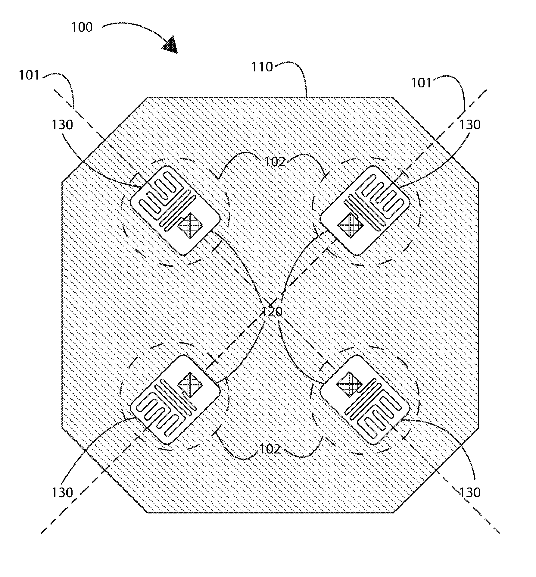
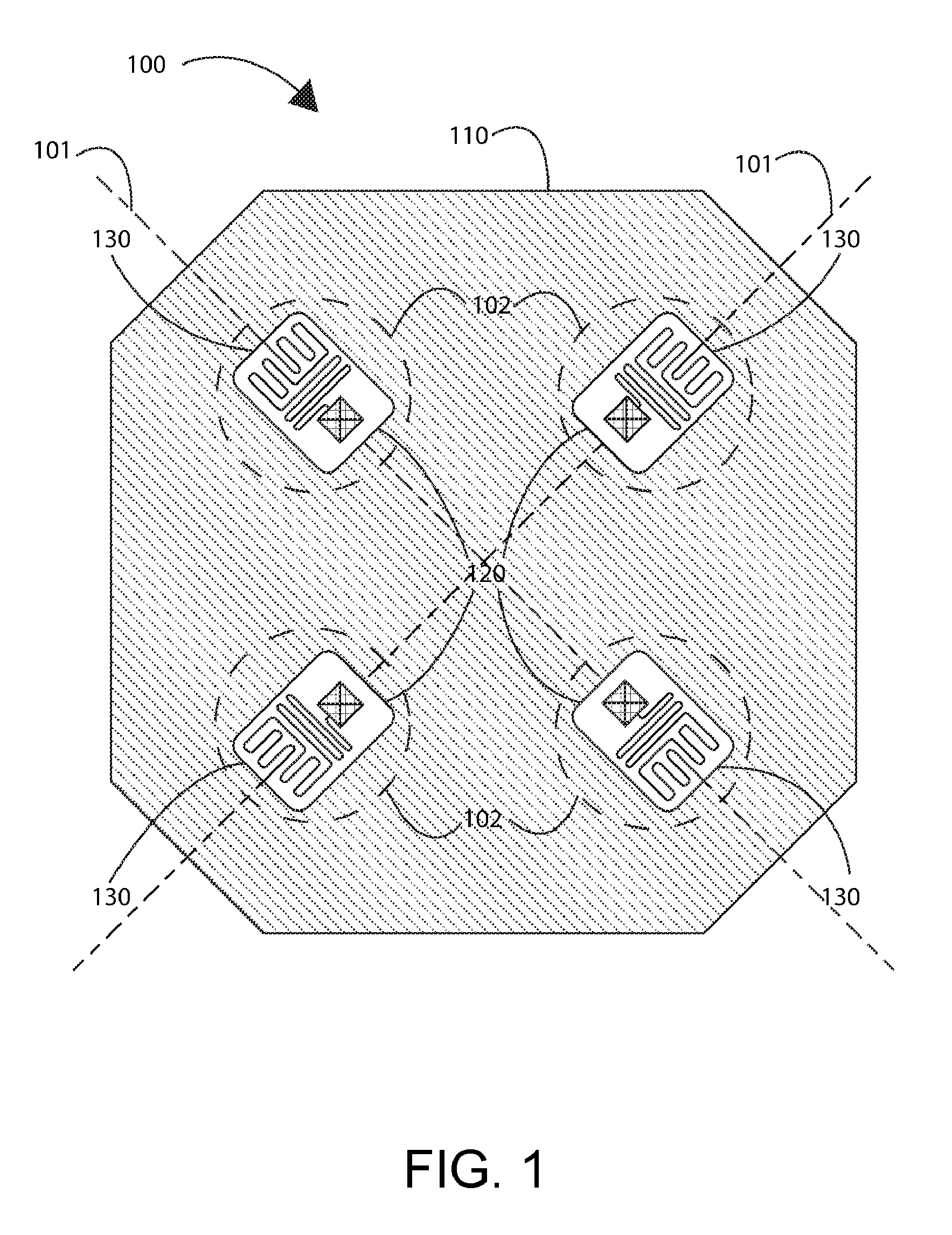
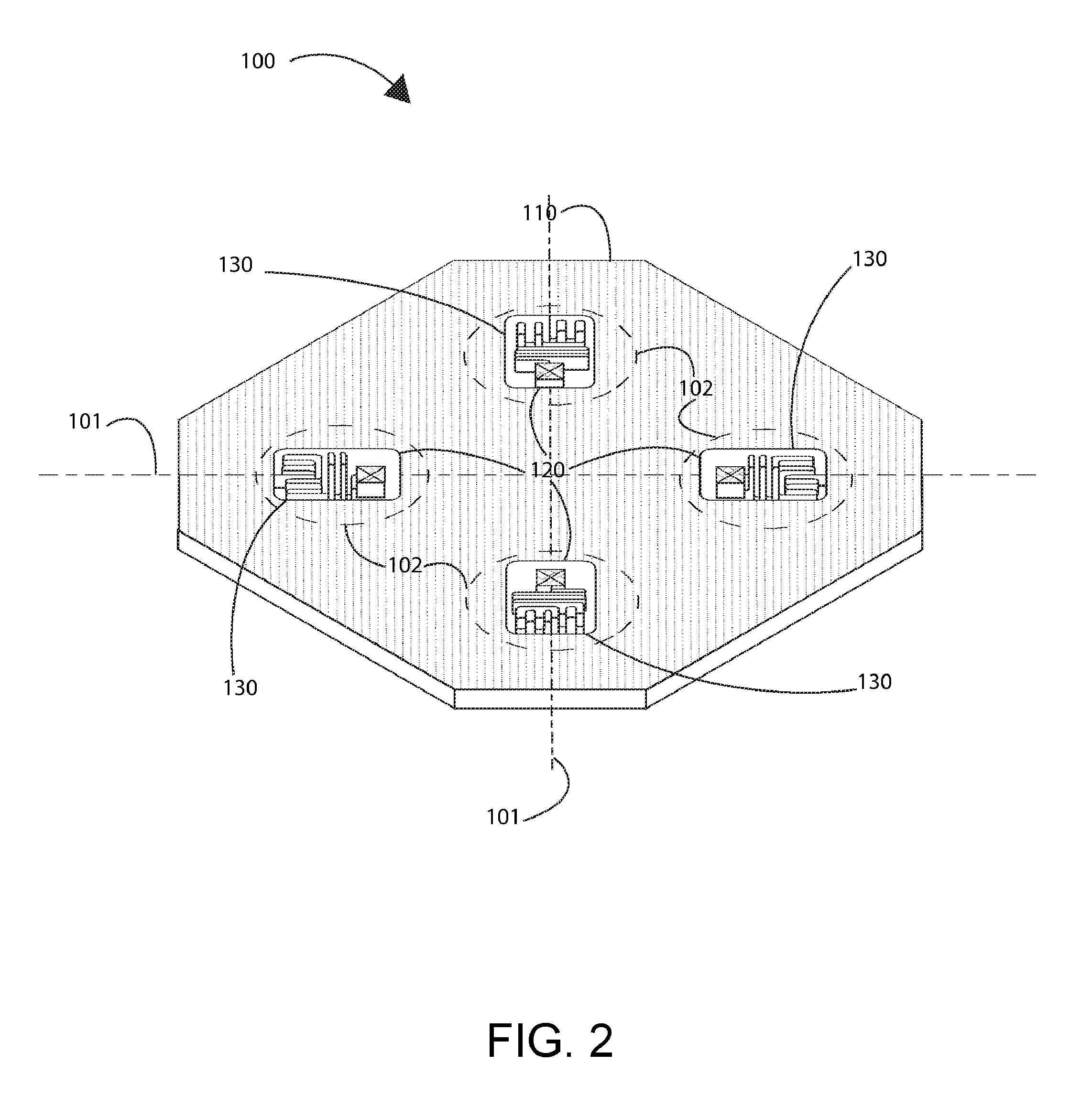
[0016]The invention provides an improved MEMS transducer apparatus that can be used with other MEMS devices, or other devices. FIG. 1 is a simplified top diagram of a transducer apparatus according to an embodiment of the present invention. As shown, apparatus 100 includes a movable base structure 110, at least one intermediate anchor structure 120, and at least one intermediate spring structure 130. In an embodiment, apparatus 100 can be configured to improve tolerance of external deformations.

[0017]In various embodiments, movable base structure 110 can have an outer surface region, and have at least one portion removed to form at least one inner surface region 102. In a specific embodiment, movable base structure 110 can be formed from a single crystal silicon, polycrystalline silicon, or amorphous silicon material. Moveable base structure 110 can also include a thickness of a polymer or a thickness of a metal material. In other embodiments, movable base structure 110 can include ...


PUM

PropertyMeasurementUnit
angleaaaaaaaaaa
orientation anglesaaaaaaaaaa
dielectricaaaaaaaaaa

Abstract

An improved MEMS transducer apparatus and method is provided. The apparatus has a movable base structure including an outer surface region and at least one portion removed to form at least one inner surface region. At least one intermediate anchor structure is disposed within the inner surface region. The apparatus includes an intermediate spring structure operably coupled to the central anchor structure, and at least one portion of the inner surface region. A capacitor element is disposed within the inner surface region.

Description

BACKGROUND OF THE INVENTION[0001]This invention relates generally to integrated devices. More specifically, the invention provides an integrated transducer apparatus that can be used in combination with other micro-electromechanical systems (MEMS) devices, but can have other uses as well. Typical MEMS devices include accelerometers, angular rate sensors, magnetic field sensors, pressure sensors, microphones, humidity sensors, temperature sensors, chemical sensors, biosensors, inertial sensors, and others.[0002]Research and development in integrated microelectronics have continued to produce progress in CMOS and MEMS technology. CMOS technology has become the predominant fabrication technology for integrated circuits (ICs). In layman's terms, ICs are the “brains” of an integrated device and provide decision-making capabilities, while MEMS are the “eyes” and “arms” and provide the ability to sense and control the environment. Some examples of the widespread application of these techno...

Claims


Application Information

Patent Timeline
Patent Type & Authority Patents(United States)
IPC IPC(8): H01G5/00
CPCG01P15/125B81B3/0072G01C19/5783G01P2015/0857B81B2203/0307B81B2203/0163Y10T29/49007G01R3/00
Inventor KOURY, JR., DANIEL N.SRIDHARAMURTHY, SUDHEER
Owner MCUBE INC
Why Eureka
Try Eureka