Thin film capacitor
a technology of thin film capacitors and film capacitors, applied in the direction of fixed capacitors, stacked capacitors, fixed capacitor details, etc., can solve the problem of peeling of the insulating resin layer on the side surface of the lower electrode, and achieve the effect of suppressing peeling and effective suppressing peeling
Active Publication Date: 2013-07-02
TDK CORPARATION
View PDF9 Cites 1 Cited by
- Summary
- Abstract
- Description
- Claims
- Application Information
AI Technical Summary
Benefits of technology
The present invention provides a thin film capacitor with a device structure that prevents peeling between an insulating film and substrate. This is achieved by adding an adhesion layer between the insulating film and dielectric film that helps to bond them together. The adhesion layer can be made of a metal thin film that oxidizes easily, which helps to prevent the dielectric film from absorbing too much oxygen and degrading. Additionally, there is an electrode lead portion that is connected to the second electrode and effectively prevents peeling between the insulating film and substrate. Overall, the invention provides a more reliable and durable thin film capacitor.
Problems solved by technology
Such a difference in thickness of the insulating resin layer affects a stress generated due to a difference between a thermal expansion coefficient of the insulating resin layer and a thermal expansion coefficient of the lower electrode, and can cause peeling of the insulating resin layer on the side surface of the lower electrode.
Method used
View moreImage
Smart ImageViewing Examples
Examples
example
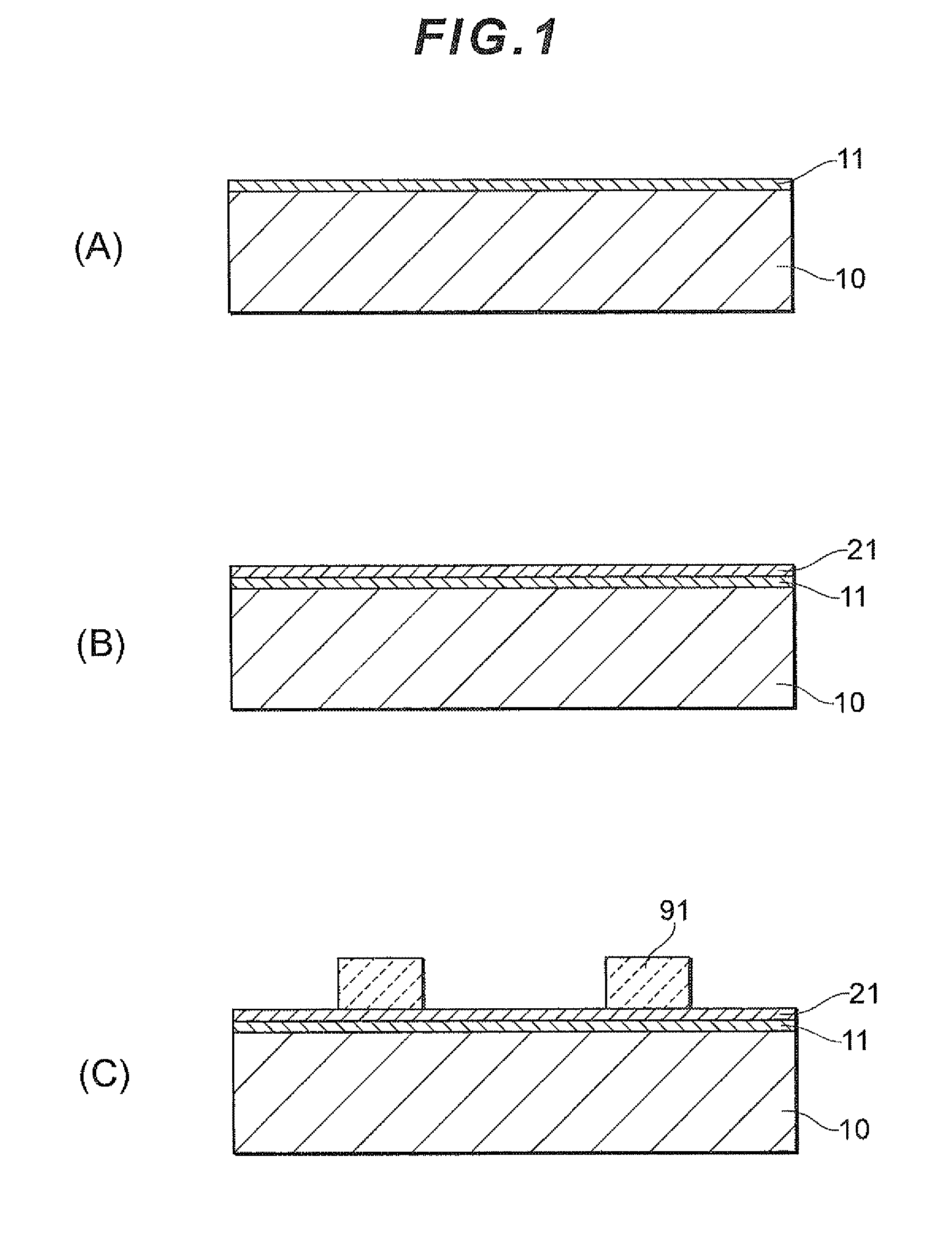
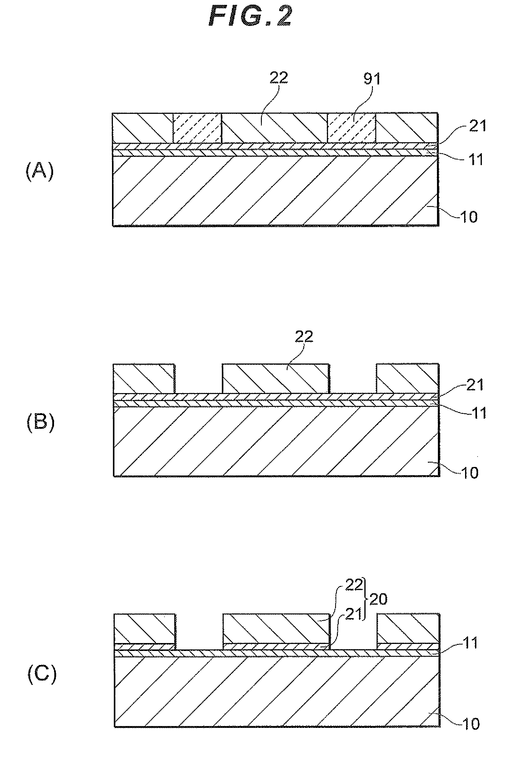
[0035]A Cu film (seed layer) was formed by sputtering on a SiNx film (dielectric film) formed by plasma CVD. A photosensitive polyimide resin (insulating film) was formed on the Cu film (seed layer) and patterned to various sizes (6 μm to 30 μm squares). PN2050 manufactured by Toray Industries, Inc. was used as the photosensitive polyimide resin. The polyimide resin (insulating film) after a developer was sprayed by showers did not peel away in any size. This result indicates favorable adhesiveness between the Cu film (seed layer) and the polyimide resin (insulating film).
Login to View More PUM
 Abstract
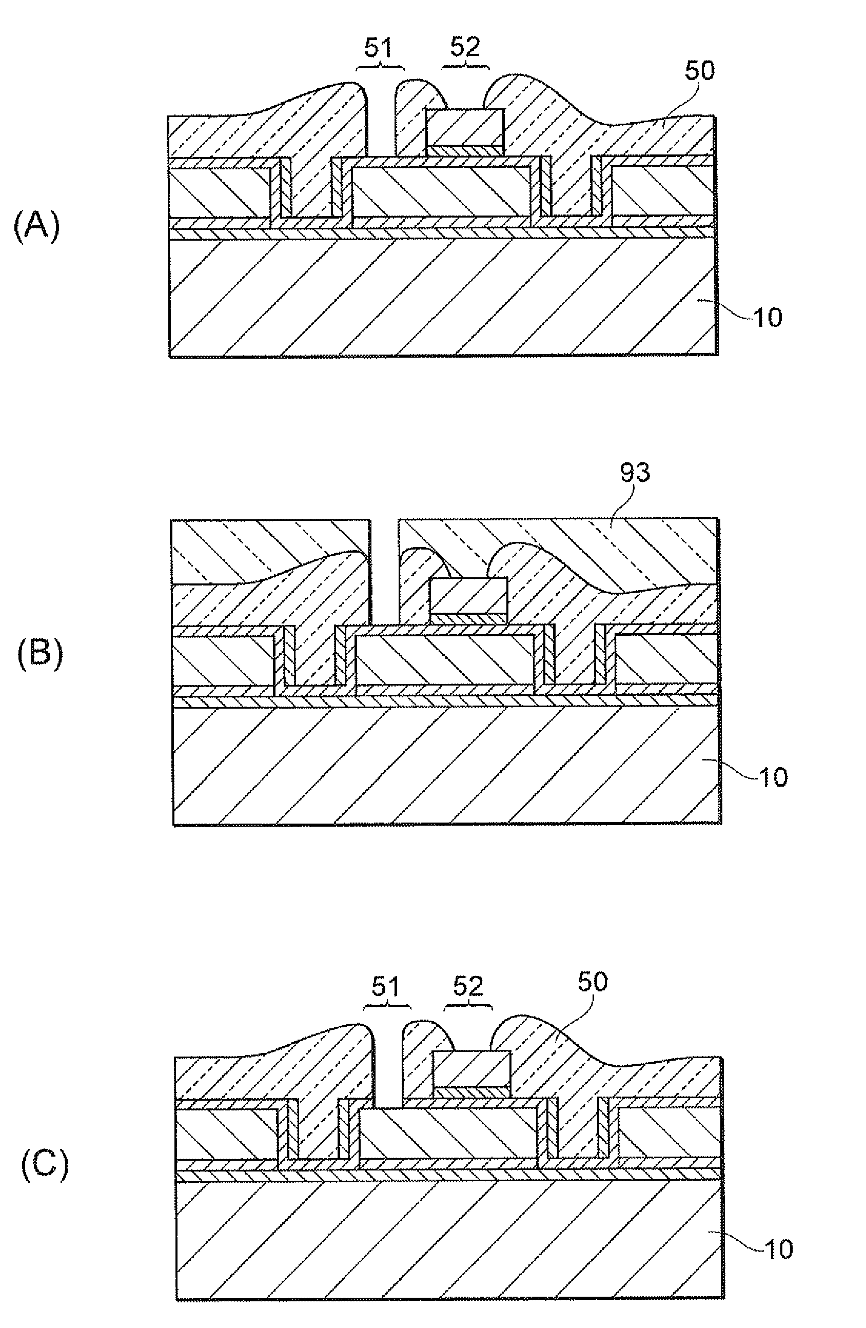
To provide a thin film capacitor having a device structure for suppressing peeling between an insulating film and a substrate. A thin film capacitor 100 has a laminate structure that is formed by laminating a lower electrode 20, a dielectric film 30, and an upper electrode 40 in sequence on a substrate 10. An adhesion layer 41 is formed on a side surface of the lower electrode 20 via the dielectric film 30, and an insulating film 50 in contact with the adhesion layer 41 covers the laminate structure. According to this device structure, the adhesion layer 41 having excellent adhesiveness to the insulating film 50 is disposed between the insulating film 50 and the dielectric film 30, so that peeling of the insulating film 50 can be suppressed.
Description
BACKGROUND OF THE INVENTION[0001]1. Field of the Invention[0002]The present invention relates to a thin film capacitor having a device structure for suppressing peeling between an insulating film and a substrate.[0003]2. Description of the Related Art[0004]A thin film capacitor is widely used in semiconductor devices, mounting circuit boards, electronic circuits, and so on. As a device structure of the thin film capacitor, various structures are being studied in light of high reliability. For example, Japanese Patent Application Laid-Open No. 2006-5293 proposes the following device structure as a device structure of a thin film capacitor having a laminate structure that is formed by laminating a lower electrode, a dielectric film, and an upper electrode in sequence on a substrate. In the proposed device structure, an insulating resin layer that has an opening for exposing the dielectric film and covers a periphery of the dielectric film is formed, and the upper electrode is laminate...
Claims
Login to View More Application Information
Patent Timeline
 Patent Type & Authority Patents(United States)
IPC IPC(8): H01G4/00H01G4/005
CPCH01G4/228H01G4/33H01L23/3142H01L23/3157H01L28/75H01L2924/19041H01L2924/0002H01L2924/00
Inventor YOSHIZAWA, TOSHIYUKIFURUYA, AKIRAISHIKURA, MASAOMITAKASUGI, KEISUKETAKE, HIROSHI
Owner TDK CORPARATION


