Organic light-emitting display panel, display device, and method of manufacturing organic light-emitting display panel

a technology of display panel and organic light, which is applied in the direction of thermoelectric device junction materials, semiconductor devices, electrical apparatus, etc., can solve the problem of difficulty in fine adjustment of the film thickness of the intermediate layers for each color, and achieve the effect of improving the luminous efficiency of each organic light-emitting elemen

Active Publication Date: 2013-07-23
JOLED INC
View PDF20 Cites 19 Cited by
  • Summary
  • Abstract
  • Description
  • Claims
  • Application Information

AI Technical Summary

Benefits of technology

[0012]The film thickness of the intermediate layers that improves luminous efficiency of each organic light-emitting element depends on the wavelength of the luminescent color. For example, in a top-emission organic light-emitting element, it is preferable that optical path lengths be set so that reflected light and direct light strengthen each other. Reflect light refers to light that is emitted from the light-emitting layer towards the substrate and reflected by an electrode or the like near the substrate before exiting through the light-emitting layer. Conversely, direct light is emitted directly upwards (in the direction opposite the substrate) from the light-emitting layer.
[0019]The present invention has been conceived in light of the above problems, and it is an object thereof to make it easy to finely adjust differences in film thickness between intermediate layers, light-emitting layers, etc. of differing luminescent colors in an organic light-emitting display panel in which such layers are formed by the wet method, thereby improving luminous efficiency, luminescent color, etc.
[0023]An organic light-emitting display panel according to an aspect of the present invention allows the depth of each first contact hole and each second contact hole to be changed by varying the thickness of the interlayer insulation film, thus making it easy to increase the volume of each first contact hole with respect to the volume of each second contact hole.
[0025]The difference between the volume of the first concavity and the volume of the second concavity can be adjusted in smaller increments than the volume of one drop of ink sprayed from a nozzle by the inkjet method. Therefore, finely adjusting the difference between the volume of the first concavity and the volume of the second concavity makes it easy to finely adjust the difference between the film thickness of the first organic functional layer and the film thickness of the second organic functional layer.
[0026]This facilitates finely adjusting the difference in film thickness between organic functional layers corresponding to different colors. As a result, it is possible, for example, to appropriately adjust the resonance conditions of light in the organic light-emitting element of each color, making it easy to achieve a display panel with excellent luminous efficiency.
[0027]Note that, in order to appropriately adjust the resonance conditions of light in the organic light-emitting element of each color, it is not necessary to adjust the optical path length only by varying the organic functional layer. The film thickness of other layers (such as a transparent electrode layer) may also be adjusted by color.

Problems solved by technology

When the wet method is used to actually form the intermediate layers, however, it is difficult to finely adjust the film thickness of the intermediate layers for each color.

Method used


Image

  • Organic light-emitting display panel, display device, and method of manufacturing organic light-emitting display panel
  • Organic light-emitting display panel, display device, and method of manufacturing organic light-emitting display panel
  • Organic light-emitting display panel, display device, and method of manufacturing organic light-emitting display panel

Examples


embodiment 1

Structure of Display Panel 100

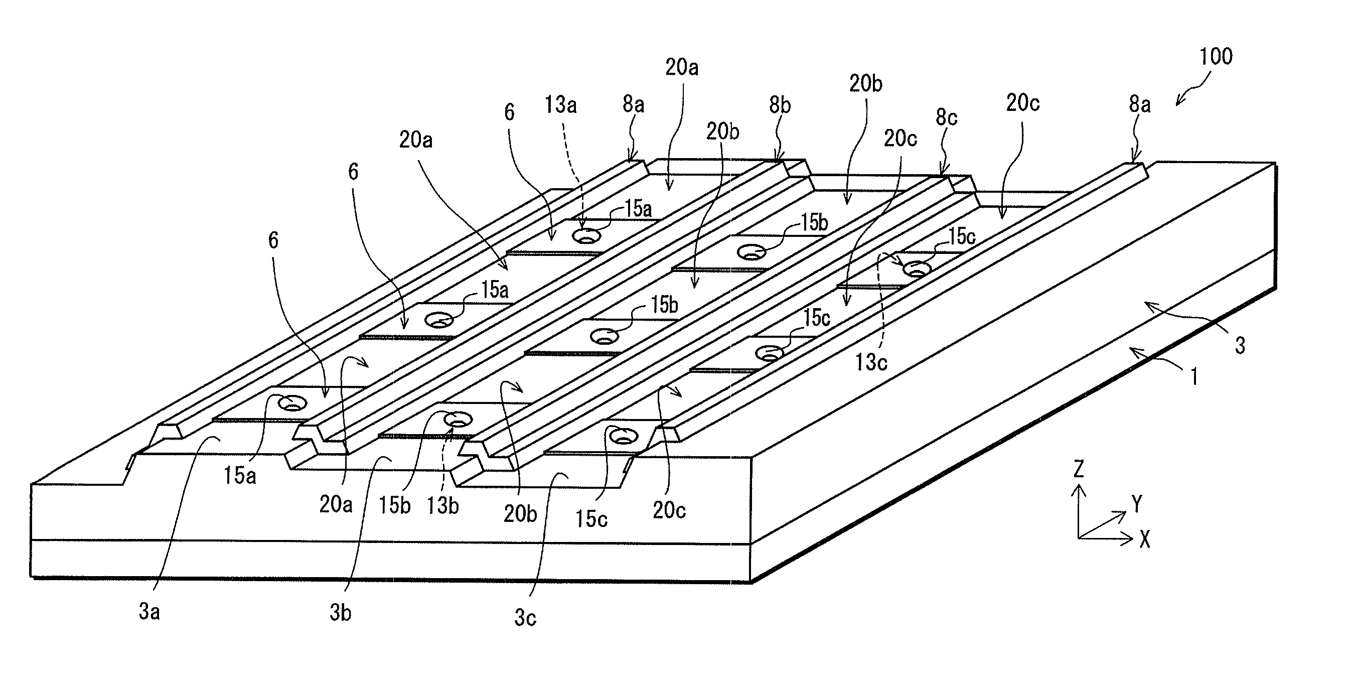
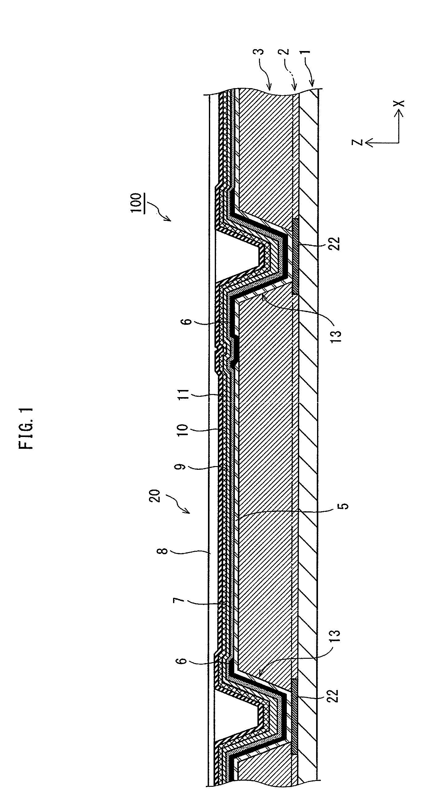
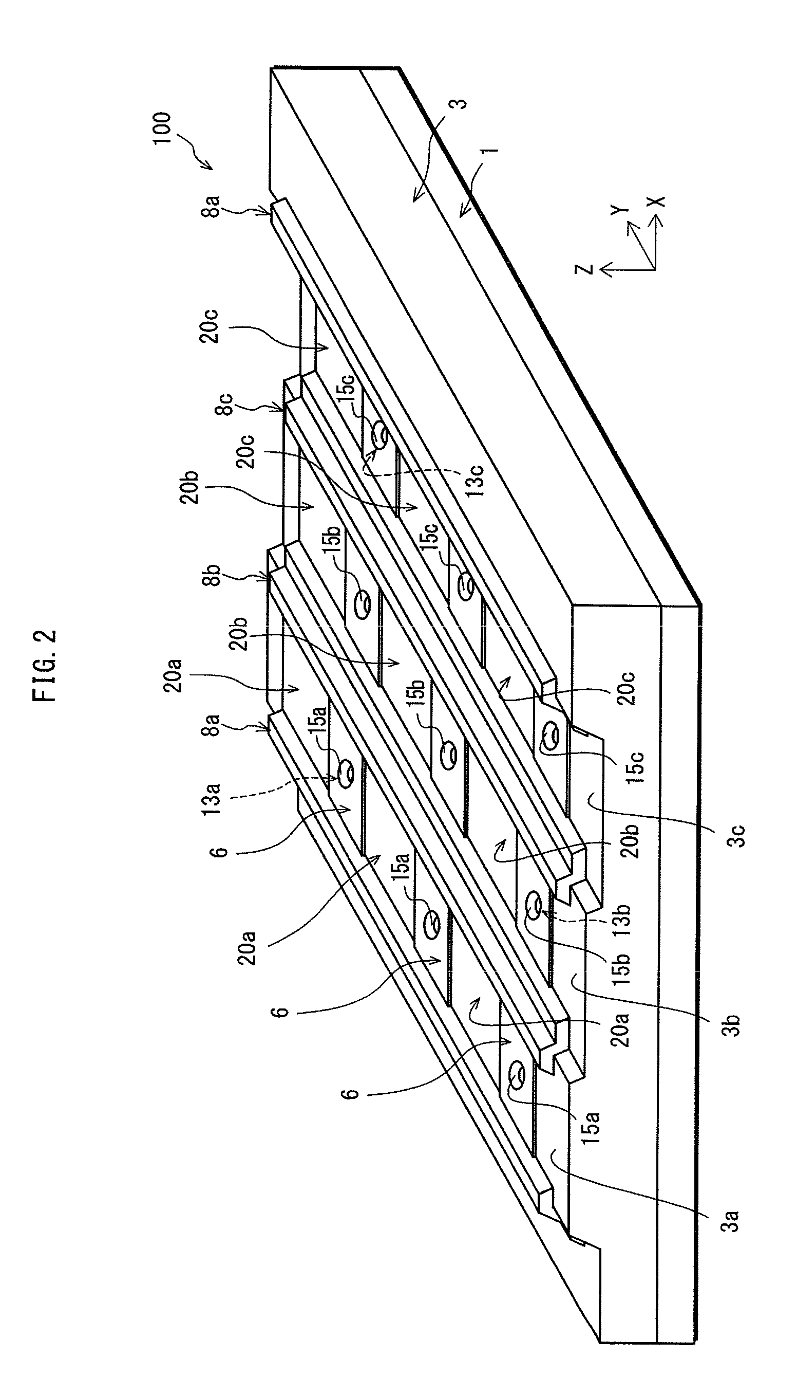
[0145]FIG. 1 is a cross-section diagram schematically showing the structure of the main parts of a display panel 100 according to Embodiment 1. FIG. 2 is a perspective view showing the structure of the main parts of the display panel 100.

[0146]The display panel unit 100 is an organic light-emitting display panel that uses the phenomenon of electroluminescence occurring in organic material. Pixels are arranged in a matrix in the lateral and longitudinal (X and Y) directions in the display panel 100. Each pixel is formed by three adjacent sub-pixels whose colors are respectively red, green, and blue (RGB). The organic light-emitting elements 20a, 20b, and 20c shown in FIG. 2 are top-emission type light-emitting elements. The organic light-emitting elements 20a are sub-pixels of a first color (blue), the organic light-emitting elements 20b are sub-pixels of a second color (green), and organic light-emitting elements 20c are sub-pixels of a third color (red...

embodiment 2

[0320]In Embodiment 1, the depth of the contact holes 13 is changed by forming levels in the interlayer insulation film 3. Alternatively, the upper surface of the interlayer insulation film may be planarized, and the height of the upper surface of the substrate where the contact hole corresponding to each color is to be formed may be changed in order to change the film thickness of the interlayer insulation film and to change the depth of the contact holes.

[0321]FIG. 11 is a cross-section diagram schematically showing a display panel 80 according to the present Embodiment. FIG. 11 shows a cross-section corresponding to the cross section A-A′ of FIG. 3A. Note that the light-emitting layer, cathode layer, etc. are omitted from FIG. 11.

[0322]In the present Embodiment, the structure shown in FIGS. 3A and 3C of Embodiment 1 is basically adopted. However, the cross-sectional shape of the substrate and of the interlayer insulation film differs. Note that the same reference numbers are used...


PUM


Abstract

An organic light-emitting display panel is provided that improves luminous efficiency and luminescent color by adjusting the difference in film thickness between layers of different luminescent colors, such as intermediate layers, when the intermediate layer and light-emitting layers are formed by a wet method. By varying the film thickness of an interlayer insulation film, which is a lower layer of an organic light-emitting element, the volume of a contact hole is varied by color, thereby adjusting the volume of a concavity in each anode plate. When ink that includes material for the intermediate layer, or like, is sprayed by an inkjet method, the film thickness of the intermediate layer, or like, changes in accordance with the amount of ink filing the concavity. Therefore, by adjusting the difference in volume between concavities of different colors, the difference in film thickness between the intermediate layers, or like, is finely adjusted.

Description

CROSS REFERENCE TO RELATED APPLICATION[0001]This is a continuation application of PCT Application No. PCT / JP2010 / 004990 filed Aug. 6, 2010, designating the United States of America, the disclosure of which, including the specification, drawings and claims, is incorporated herein by reference in its entirety.BACKGROUND OF THE INVENTION[0002]1. Field of the Invention[0003]The present invention relates to organic light-emitting display panels containing a matrix of organic light-emitting elements, to display devices, and to methods of manufacturing organic light-emitting display panels.[0004]2. Description of the Related Art[0005]In recent years, organic light-emitting display panels that have a plurality of organic light-emitting elements in rows above a substrate have been used as light-emitting display panels in compact electronic equipment and compact display devices. The basic structure of an organic light-emitting element is to form a light-emitting layer, which includes organic ...

Claims


Application Information

Patent Timeline
Patent Type & Authority Patents(United States)
IPC IPC(8): H01L35/24H01L21/00
CPCH01L51/5265H01L27/3258H01L27/3248H01L27/3211H01L27/3246H10K59/35H10K59/122H10K59/123H10K59/124H10K50/852H10K71/135H10K10/46
Inventor NISHIYAMA, SEIJIKONDOH, TETSURO
Owner JOLED INC
Why Eureka
Try Eureka