Method and apparatus for high resolution photon detection based on extraordinary optoconductance (EOC) effects

a technology of optoconductance and high-resolution photons, applied in the direction of cathode ray tubes/electron beam tubes, instruments, radio-controlled devices, etc., can solve the problem that nanowire-based nanophotonic devices are not currently compatible with very/ultra large-scale integration (vlsuulsi) fabrication methods, and achieve significant sensitivity in the visible light spectrum

Active Publication Date: 2013-07-30
WASHINGTON UNIV IN SAINT LOUIS
View PDF33 Cites 6 Cited by
  • Summary
  • Abstract
  • Description
  • Claims
  • Application Information

AI Technical Summary

Benefits of technology

[0013]In accordance with another aspect of an embodiment of the present invention, the inventors herein disclose a method that comprises perturbing a nanoscale MSH device having a semiconductor / metal interface that defines a Schottky barrier (non-linear) interface with light to produce an I-EOC effect.

Problems solved by technology

Moreover, although much work on nanowire-based nanophotonic devices have been reported, the inventors believe that such nanowire-based nanophotonic devices are not currently compatible with Very / Ultra Large Scale Integration (VLSUULSI) fabrication methods.

Method used


Image

  • Method and apparatus for high resolution photon detection based on extraordinary optoconductance (EOC) effects
  • Method and apparatus for high resolution photon detection based on extraordinary optoconductance (EOC) effects
  • Method and apparatus for high resolution photon detection based on extraordinary optoconductance (EOC) effects

Examples


Embodiment Construction

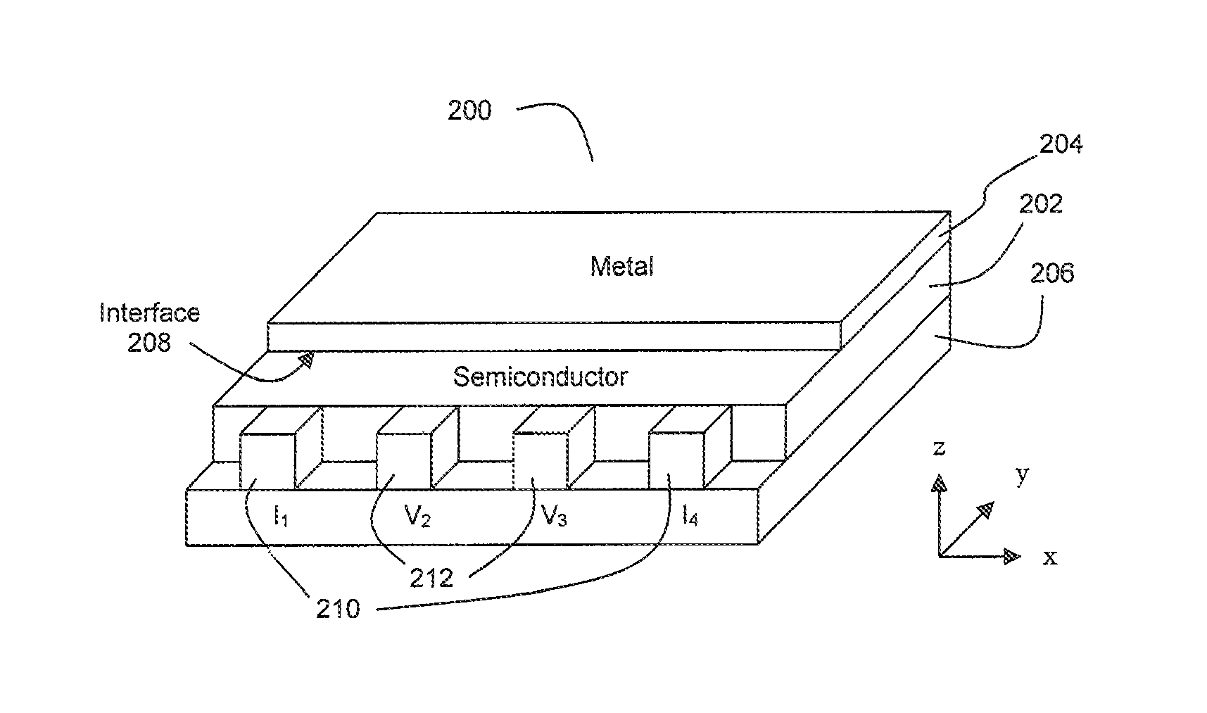
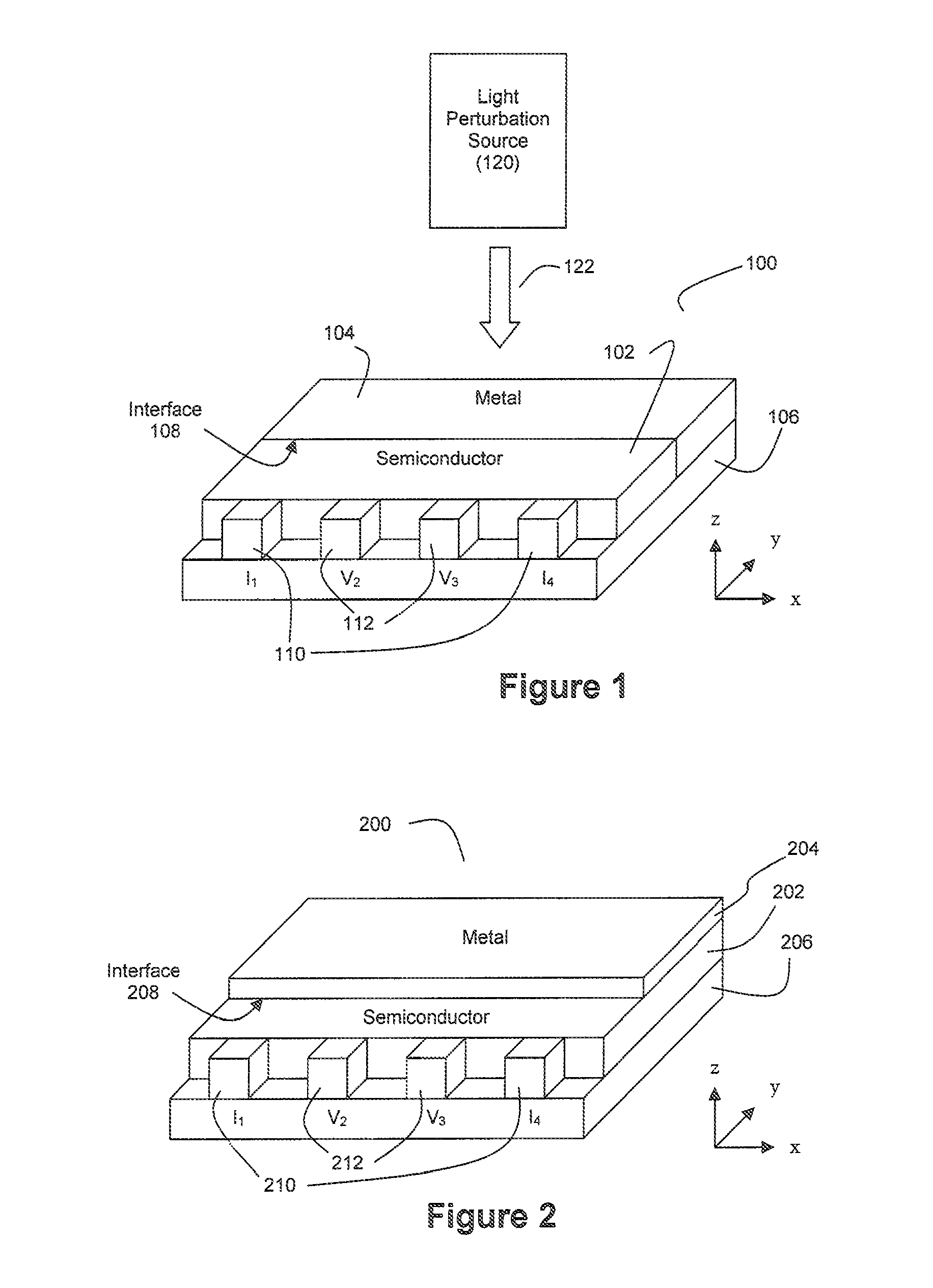
[0034]FIG. 4 depicts an exemplary MSH device 200 that can be employed as an EOC sensor in accordance with an embodiment of the present invention. As shown in FIG. 4, the EOC sensor 200 is an MSH device comprising several layers, including a semiconductor portion 202 and a metal shunt portion 204. The metal shunt portion 204 is disposed on a surface of the semiconductor portion 202, and the semiconductor portion 202 is disposed on a surface of substrate 206 such that the semiconductor portion 204 is sandwiched between the metal shunt portion 202 and the substrate 206. As shown in FIG. 4, the metal shunt portion 204, the semiconductor portion 202, and the substrate portion 206 preferably lie in substantially parallel planes. Together, the contact between the metal shunt portion 204 and the semiconductor portion 206 define a semiconductor / metal interface 208. Thus, unlike the EOC sensor architecture described in the related and above-referenced patent applications, the plane of the sem...


PUM


Abstract

The inventors disclose a new high performance optical sensor, preferably of nanoscale dimensions, that functions at room temperature based on an extraordinary optoconductance (EOC) phenomenon, and preferably an inverse EOC (I-EOC) phenomenon, in a metal-semiconductor hybrid (MSH) structure having a semiconductor / metal interface. Such a design shows efficient photon sensing not exhibited by bare semiconductors. In experimentation with an exemplary embodiment, ultrahigh spatial resolution 4-point optoconductance measurements using Helium-Neon laser radiation reveal a strikingly large optoconductance property, an observed maximum measurement of 9460% EOC, for a 250 nm device. Such an exemplary EOC device also demonstrates specific detectivity higher than 5.06×1011 cm√Hz / W for 632 nm illumination and a high dynamic response of 40 dB making such sensors technologically competitive for a wide range of practical applications.

Description

CROSS-REFERENCE AND PRIORITY CLAIM TO RELATED PATENT APPLICATIONS[0001]This patent application claims priority to U.S. provisional patent application Ser. No. 61 / 293,442; filed Jan. 8, 2010, the entire disclosure of which is incorporated herein by reference.[0002]This patent application is related to pending U.S. patent application Ser. No. 12 / 375,861, filed Jan. 30, 2009, which is a U.S. national phase entry of PCT patent application PCT / US07 / 74864, filed Jul. 31, 2007, which claims priority to U.S. provisional patent application 60 / 821,040, filed Aug. 1, 2006, the entire disclosures of each of which are incorporated herein by reference.BACKGROUND AND SUMMARY OF THE INVENTION[0003]Extraordinary optoconductance (EOC) is a recent example of a class of geometry-driven interfacial “EXX” phenomena exhibited by metal-semiconductor hybrid (MSH) structures, wherein:[0004]E=extraordinary; and[0005]XX=a type of interfacial phenomena such as magnetoresistance (MR), piezoconductance (PC), opto...

Claims


Application Information

Patent Timeline
Patent Type & Authority Patents(United States)
IPC IPC(8): H01J29/02H01J40/14
CPCH01L27/14665H01L31/0304H01L31/09H01L31/108H01L27/1446Y02E10/544B82Y15/00H01L31/08
Inventor SOLIN, STUART A.WICKLINE, SAMUEL A.NEWAZ, AKM SHAHWALLACE, KIRK D.
Owner WASHINGTON UNIV IN SAINT LOUIS
Why Eureka
Try Eureka