On-chip sensor for measuring dynamic power supply noise of the semiconductor chip

a technology of dynamic power supply noise and on-chip sensor, which is applied in the field of voltage sensors, can solve the problems of high operational delay, large amount of time required for performing the operation, and often present dynamic power supply noise in the circuitry, so as to improve the sensitivity of the in-situ probe's operational delay, avoid extra pin overhead, and accurate functional logic performance

Active Publication Date: 2013-07-30
QUALCOMM INC
View PDF16 Cites 19 Cited by
  • Summary
  • Abstract
  • Description
  • Claims
  • Application Information

AI Technical Summary

Benefits of technology

[0013]According to embodiments of the present disclosure, an on-chip sensor is proposed for capturing the dynamic power supply noise behavior for the chip. The chip has functional logic for performing the operations for the target application of the chip, and sensor logic that is added on the chip for monitoring the dynamic power supply noise of the chip. In this way, the on-chip sensor logic can monitor the dynamic power supply noise of the chip to determine a behavioral profile for the power supply noise that can be used for maintaining accurate performance of the functional logic.
[0015]During operation, the functional logic functions as normal, such as it would for an intended application. For instance, a microprocessor in the noisy power portion may execute instructions of a given software application. As is normal, the functional logic (e.g., microprocessor) performs its operations with reference to a reference clock signal. A separate delayed clock signal, having some controlled delay amount (or “delta”) relative to the reference clock signal, is supplied to the in-situ probe portion. The in-situ probe portion performs some operation based on the delayed clock signal, and returns an output signal. In one embodiment, the in-situ probe portion has a series of inverters to generate an inverted delay signal. As is discussed further herein, in one embodiment stacked inverters are employed to improve the sensitivity of the in-situ probe's operational delay to voltage fluctuation. In one exemplary embodiment, five stacked inverters are employed for the in-situ probe. Since the probing portion implemented in this manner consumes a small area, it can be efficiently embedded into standard library cell logic blocks.
[0023]As described above, the in-situ probing portion of certain embodiments contains voltage droop information. To use only digital input / output (I / O), this delay is to be converted to a digital signal. In certain embodiments, the delay is changed to a control signal of the variable delay block. Variable delay is increased with control signal incrementally. When the probing portion delay is matched to the delay of the variable delay, the control signal can be read. In this way, the probing delay can be converted to a digital signal efficiently.
[0025]According to certain embodiments, a sensor is provided that can be implemented in a relatively small area such that it can be efficiently embedded in a standard cell logic block. Also, in certain embodiments, a sensor is provided that employs fully digital signals as I / O signals, which means that the sensor is robust to aliasing noise of the output pad. Further, in certain embodiments, statistical methods are employed to overcome jitter and circuit uncertainty.

Problems solved by technology

The in-situ logic performs some operation, and the amount of time required for performing that operation (i.e., the operational delay) is sensitive to noise present on the power supply.
Accordingly, dynamic power supply noise for the circuitry is often present around the rising or falling edges of the reference clock signal.

Method used


Image

  • On-chip sensor for measuring dynamic power supply noise of the semiconductor chip
  • On-chip sensor for measuring dynamic power supply noise of the semiconductor chip
  • On-chip sensor for measuring dynamic power supply noise of the semiconductor chip

Examples


Embodiment Construction

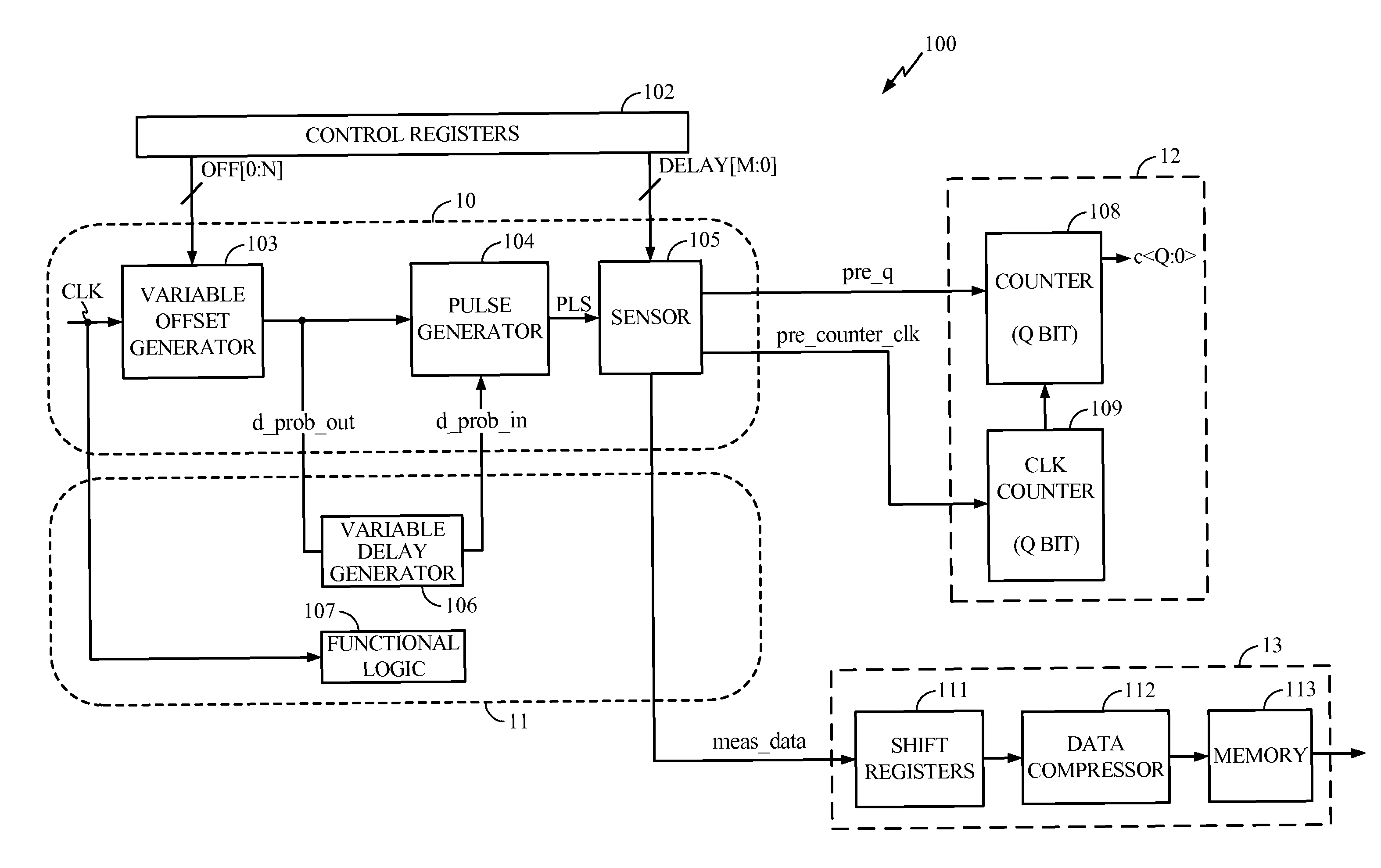
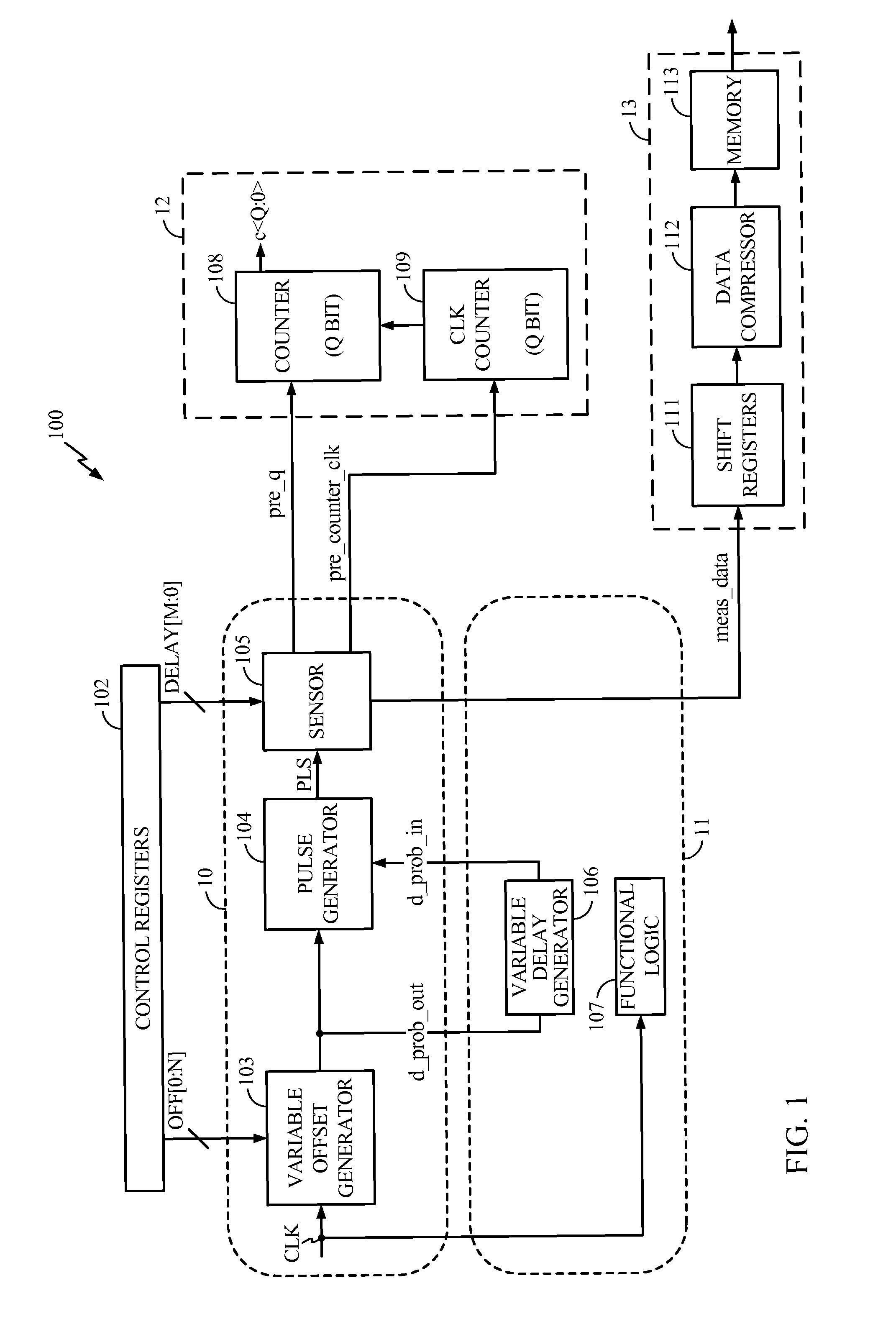
[0053]FIG. 1 is a block diagram illustrating an exemplary on-chip sensor according to one embodiment of the present disclosure. In this example, an on-chip architecture 100 includes a clean power area 10 and a noisy power area 11. The noisy power area 11 includes the functional logic 107 of an integrated circuit. This may be, for example, a processor core or other logic circuitry in which dynamic power supply noise is measured by the on-chip sensor 100. The functional logic 107 introduces noise into the noisy power area 11 when transistors switch on and off causing voltage droop as described above. A variable delay generator 106 is included in the noisy power area 11 of the chip and shares power with the functional logic 107. As a result, the variable delay generator 106 is subject to the same power noise as the functional logic 107. The clean power area 10 includes separate power and ground lines (not shown) for use by a variable offset generator 103, a pulse generator 104, and a s...


PUM


Abstract

An on-chip sensor measures dynamic power supply noise, such as voltage droop, on a semiconductor chip. In-situ logic is employed, which is sensitive to noise present on the power supply of functional logic of the chip. Exemplary functional logic includes a microprocessor, adder, and / or other functional logic of the chip. The in-situ logic performs some operation, and the amount of time required for performing that operation (i.e., the operational delay) is sensitive to noise present on the power supply. Thus, by evaluating the operational delay of the in-situ logic, the amount of noise present on the power supply can be measured.

Description

TECHNICAL FIELD[0001]The following description relates generally to voltage sensors, and more particularly to an on-chip sensor for detecting dynamic power supply noise, such as voltage droop, encountered during operation of a semiconductor chip.BACKGROUND[0002]Power supply noise in integrated circuits (ICs) (wherein the terms “IC,”“chips,”“semiconductor chips” are used synonymously throughout this specification) has emerged as a critical issue, particularly in sub-100 nanometer (nm) technology. Power supply noise causes fluctuations in the voltage differences between power supply and ground rails within ICs resulting in unpredictable timing violations or logical event failures. Certain design flows that manage power supply noise rely on power analysis tools based on highly capable, fast transistor-level or abstracted gate-level simulations. How accurately such simulations can predict noises in terms of amplitudes, timings, and locations within a circuit, however, is largely unknown...

Claims


Application Information

Patent Timeline
Patent Type & Authority Patents(United States)
IPC IPC(8): G01R31/36G01R31/3187
CPCG01R29/26G01R31/31721
Inventor CHUA-EOAN, LEWANDREEV, BORISPHAN, CHRISTOPHERSHAYAN, AMIRALIKONG, XIAOHUAPOPOVICH, MIKHAILCALLE, MAURICIOCHANG, IK-JOON
Owner QUALCOMM INC
Why Eureka
Try Eureka