Supercharge Your Innovation With Domain-Expert AI Agents!

Integrating Schottky diode into power MOSFET

a technology of schottky diodes and power mosfets, which is applied in the direction of diodes, semiconductor devices, electrical apparatus, etc., can solve the problems of large recovery current and voltage overshoots, undesirable characteristics of typical p-n junction diodes, and lower conduction loss

Active Publication Date: 2013-08-06
ALPHA & OMEGA SEMICON INC
View PDF53 Cites 9 Cited by
  • Summary
  • Abstract
  • Description
  • Claims
  • Application Information

AI Technical Summary

Benefits of technology

The patent presents a way to make integrated structures that include power MOSFET devices and Schottky diodes. This method allows for the use of Schottky diodes without adding too much extra expense or complexity to the fabrication process. The result is better device performance and lower costs.

Problems solved by technology

However, typical P-N junction diodes exhibit undesirable characteristics during operation.
These undesirable characteristics include: large forward conduction loss, storage of charge between body-epitaxial junction when operating in forward bias, excess stored minority charges which cause large recovery currents and voltage overshoots when the power MOSFET is switched from forward bias to reverse bias, and phase node voltage overshooting / ringing when implemented in a DC-DC converter application.
The low forward drop of the Schottky diode during forward conduction reduces power dissipation of the device and leads to lower conduction loss.

Method used


Image

  • Integrating Schottky diode into power MOSFET
  • Integrating Schottky diode into power MOSFET
  • Integrating Schottky diode into power MOSFET

Examples


Embodiment Construction

[0015]A detailed description of one or more embodiments of the invention is provided below along with accompanying figures that illustrate the principles of the invention. The invention is described in connection with such embodiments, but the invention is not limited to any embodiment. The scope of the invention is limited only by the claims and the invention encompasses numerous alternatives, modifications, and equivalents. Numerous specific details are set forth in the following description in order to provide a thorough understanding of the invention. These details are provided for the purpose of example and the invention may be practiced according to the claims without some or all of these specific details. For the purpose of clarity, technical material that is known in the technical fields related to the invention has not been described in detail so that the invention is not unnecessarily obscured.

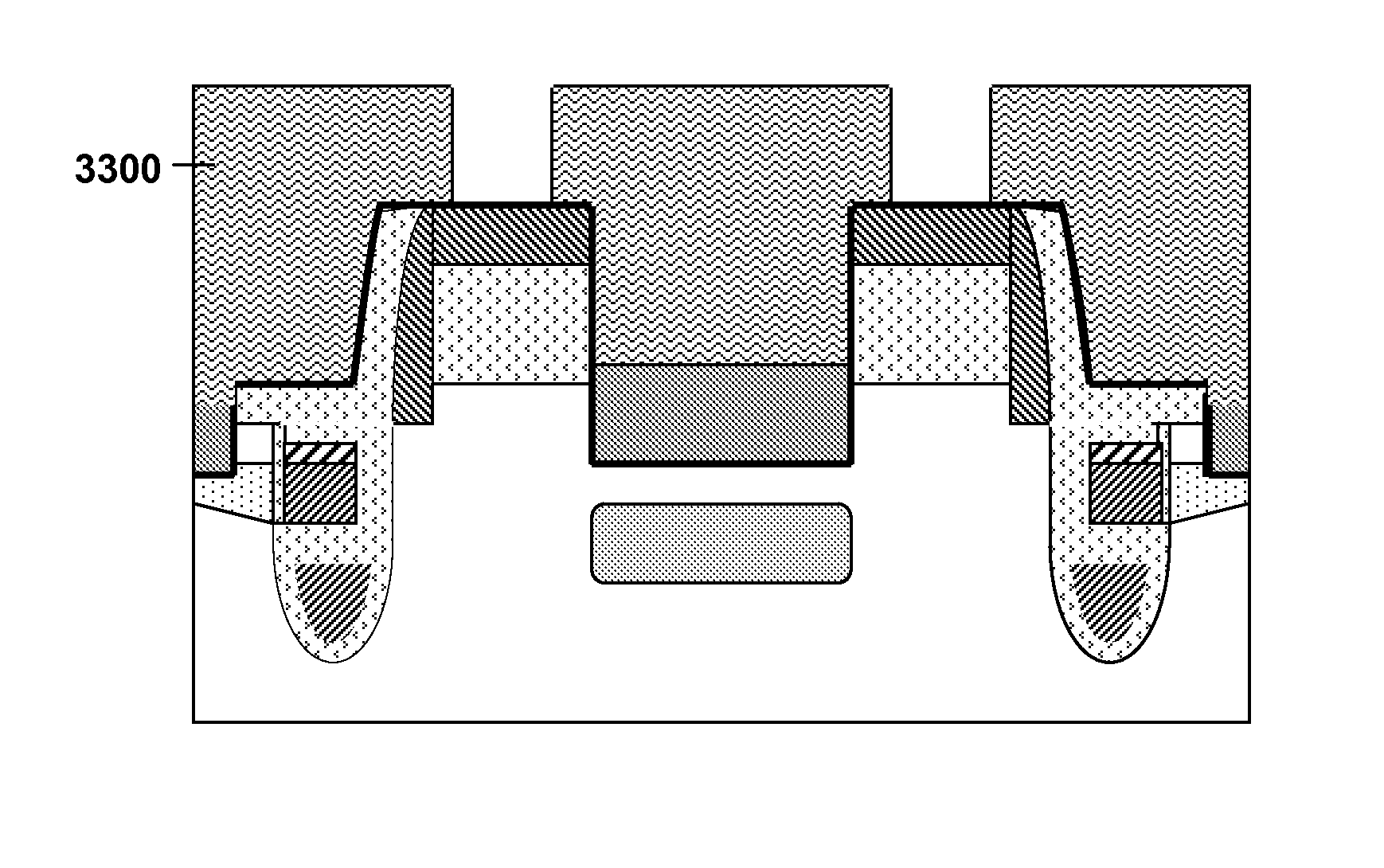
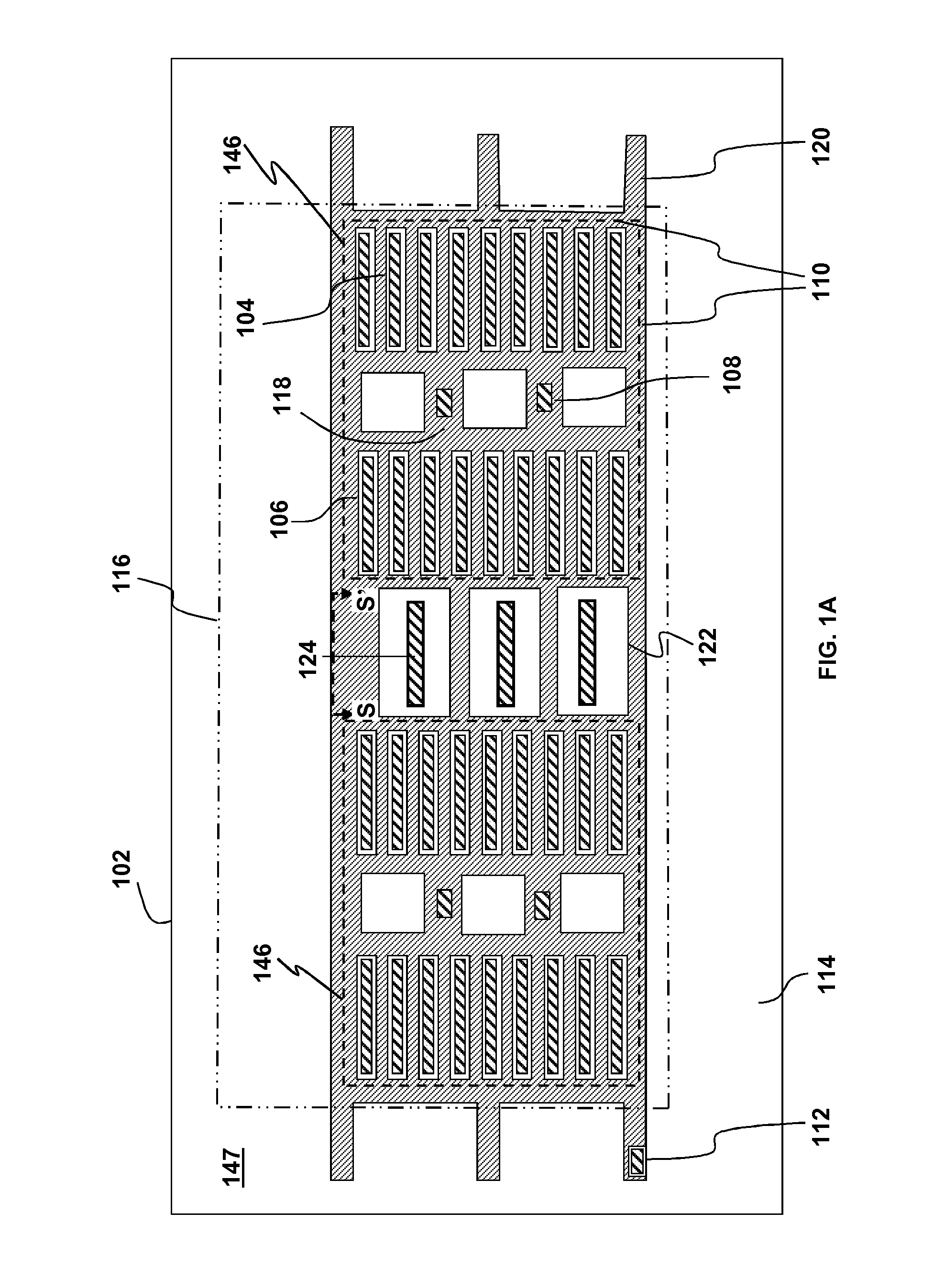
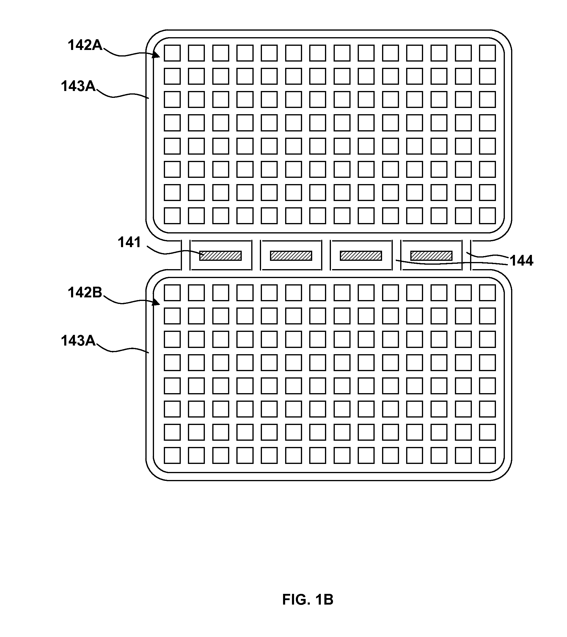
[0016]Embodiments of the integrated structure comprising power MOSFET devices im...


PUM


Abstract

A semiconductor device includes a plurality of trenches including active gate trenches in an active area and gate runner / termination trenches and shield electrode pickup trenches in a termination area outside the active area. The gate runner / termination trenches include one or more trenches that define a mesa located outside an active area. A first conductive region is formed in the plurality of trenches. An intermediate dielectric region and termination protection region are formed in the trenches that define the mesa. A second conductive region is formed in the portion of the trenches that define the mesa. The second conductive region is electrically isolated from the first conductive region by the intermediate dielectric region. A first electrical contact is made to the second conductive regions and a second electrical contact to the first conductive region in the shield electrode pickup trenches. One or more Schottky diodes are formed within the mesa.

Description

FIELD OF THE INVENTION[0001]This invention generally relates to semiconductor devices and more particularly to the methods for fabricating shielded gate trench MOS with an integrated Schottky diode within the termination region.BACKGROUND OF INVENTION[0002]A method for fabricating a semiconductor device using only four masks is disclosed in U.S. patent application Ser. No. 12 / 722,384 filed Mar. 11, 2010, entitled “SHIELDED GATE TRENCH MOS WITH IMPROVED SOURCE PICKUP LAYOUT”, the entire contents of which are incorporated herein by reference. The method includes forming a plurality of trenches by applying a first mask, forming a first conductive region in the plurality of trenches, forming an intermediate dielectric region and a termination protection region by applying a second mask, forming a second conductive region in at least some of the trenches, forming a first electrical contact to the second conductive regions and forming a second electrical contact to the first conductive re...

Claims


Application Information

Patent Timeline
Patent Type & Authority Patents(United States)
IPC IPC(8): H01L27/06H01L21/336
CPCH01L29/872H01L29/407H01L29/66719H01L29/66727H01L29/66734H01L29/7806H01L29/7811H01L29/7813H01L29/782H01L29/78H01L29/0696H01L21/26586H01L29/41766H01L29/42368H01L29/4238H01L29/47H01L29/4933H01L29/0623H01L29/7801H01L29/0891
Inventor SU, YING, DANIELBHALLA, ANUPCHANG, HONGKIM, JONGOHCHEN, JOHN
Owner ALPHA & OMEGA SEMICON INC
Features
  • R&D
  • Intellectual Property
  • Life Sciences
  • Materials
  • Tech Scout
  • Unparalleled Data Quality
  • Higher Quality Content
  • 60% Fewer Hallucinations
Learn More