Method for forming metal gate and MOS transistor

a technology of metal gate and mos transistor, which is applied in the direction of basic electric elements, electrical equipment, semiconductor devices, etc., can solve the problems of deterioration of electrical performance, affecting the performance of metal gates, and affecting the reliability of electrical components, so as to avoid deterioration of electric performance and reliability

Active Publication Date: 2013-08-13
SEMICONDUCTOR MANUFACTURING INTERNATIONAL (BEIJING) CORP
View PDF8 Cites 1 Cited by
  • Summary
  • Abstract
  • Description
  • Claims
  • Application Information

AI Technical Summary

Benefits of technology

[0013]Embodiments of the present invention provide a method for forming a metal gate and a method for forming a MOS transistor, which prevent from metal bridge and metal residuals, and correspondingly avoiding deterioration of electric performance and reliability of a semiconductor device.
[0059]In the present invention, before removing the polysilicon gate, a first part of the stop layer parallel to the substrate on the spacers and the polysilicon gate is removed. A predetermined thickness of the second part of the stop layer in the spacers is removed. The predetermined thickness corresponds to the thickness of the sacrificial oxide layer. A second interlayer dielectric layer is formed on the first interlayer dielectric layer that covers the spacers and the polysilicon gate. The second interlayer dielectric layer is polished to expose the polysilicon gate. The polysilicon gate and the sacrificial oxide layer are removed. The second interlayer dielectric layer is substantially flush with the silicon oxide layer in the spacers and the polysilicon gate. In a subsequent process, the metal layer is polished by CMP process to form a metal gate. The metal layer is not remained in the interlayer dielectric layer. Recesses, and therefore metal bridge and metal residuals in the recesses, are avoided. Correspondingly, shortcut is avoided effectively, and electric performance and reliability is promoted.

Problems solved by technology

This step may impact performance of the metal gate formed in a subsequent step.
Shortcut may occur, resulting in deterioration of performance.
Shortcut may occur, tending to cause deterioration of electrical performance.

Method used


Image

  • Method for forming metal gate and MOS transistor
  • Method for forming metal gate and MOS transistor
  • Method for forming metal gate and MOS transistor

Examples


embodiment i

[0082]FIGS. 8-15 are cross-sectional views of intermediate structures of a metal gate, illustrating a method for forming the metal gate according to an embodiment of the present invention. As shown in FIG. 8, a substrate 100 is provided. A sacrificial oxide layer 101 and a polysilicon gate 102 are formed on the substrate 100 in sequence. A silicon oxide layer 103 is formed on sidewalls of the polysilicon gate 102 and the sacrificial oxide layer 101. A stop layer 104 is formed on the substrate 100 and covers the silicon oxide layer 103 and the polysilicon gate 102. The stop layer 104 includes a first part 1042 on the silicon oxide layer 103 and the polysilicon gate 102, and a second part 1041 on opposite sides of the polysilicon gate 102. The second part 1041 of the stop layer 104 and the silicon oxide layer 103 constitute spacers. A first interlayer dielectric layer 105a is formed on the stop layer 104 for covering the spacers and the polysilicon gate 102.

[0083]In an exemplary embod...

embodiment

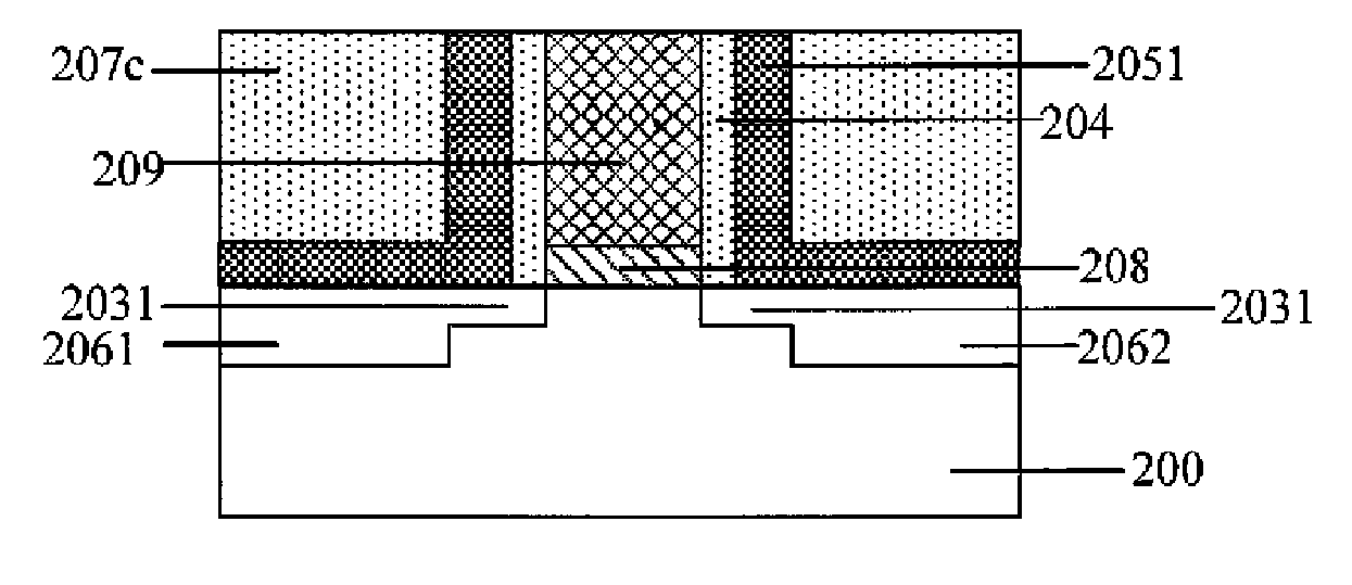
[0101]FIGS. 16-24 are cross-sectional views of intermediate structures of a MOS transistor, illustrating a method for forming a MOS transistor according to an embodiment of the present invention.

[0102]As shown in FIG. 16, a substrate 200 is provided. A sacrificial oxide layer 201 and a polysilicon gate 202 are formed on the substrate 200 in sequence. A light dopant region 203 is formed in the substrate 200 and at opposite sides of the polysilicon gate 202. In one specific embodiment, a sacrificial oxide layer 201 is formed on the substrate 200 by hot oxidation, for example tube hot oxidation. A first photoresist layer (not shown) is formed on the sacrificial oxide layer 201, and defines an n-well pattern or p-well pattern thereon after exposure and development. Taking the first photoresist layer as a mask, the substrate 200 is doped by ion implantation for forming a MOS well (not shown). The first photoresist layer is removed for forming a polysilicon layer on the sacrificial oxide...


PUM

PropertyMeasurementUnit
dielectric constantaaaaaaaaaa
diameteraaaaaaaaaa
particle diameteraaaaaaaaaa

Abstract

The invention provides a method for forming a metal gate and a method for forming a MOS transistor. The method for forming a metal gate includes: providing a substrate; forming a sacrificial oxide layer and a polysilicon gate on the substrate; forming a silicon oxide layer on sidewalls of the sacrificial oxide layer and the polysilicon gate; forming a stop layer that covers the substrate; removing a part of the stop layer in the spacers; forming a second interlayer dielectric layer that covers the first interlayer dielectric layer, the spacers and the polysilicon gate; polishing the second interlayer dielectric layer to expose the spacers and the polysilicon gate; removing the polysilicon gate to form a trench; removing the sacrificial oxide layer in the trench; and forming a metal gate in the trench. The invention prevents from recesses and therefore metal bridge and metal residuals in the recesses.

Description

CROSS REFERENCE TO RELATED APPLICATIONS[0001]The present application claims the priority of Chinese Patent Application No. 201010571163.7, entitled “METAL GATE AND METHOD FOR FORMING MOS TRANSISTOR”, and filed Dec. 2, 2010, the entire disclosure of which is incorporated herein by reference.BACKGROUND OF THE INVENTION[0002]1. Field of the Invention[0003]The present invention generally relates to the field of semiconductor manufacture, and particularly to a method for forming a metal gate and a method for forming a MOS transistor.[0004]2. Description of Prior Art[0005]In the wake of an ever increasing integration level of semiconductor devices, in a mainstream method for fabricating MOS transistor for advanced semiconductor device, a gate dielectric layer includes high k material with dielectric constant of no less than 10, and a metal gate includes metal material. When a metal gate is formed on a high k gate dielectric layer, a step of polishing interlayer dielectric layer (ILD) is n...

Claims


Application Information

Patent Timeline
Patent Type & Authority Patents(United States)
IPC IPC(8): H01L21/336H01L21/28
CPCH01L29/6653H01L29/66545H01L29/7833H01L21/31053
Inventor JIANG, LILI, MINGQI
Owner SEMICONDUCTOR MANUFACTURING INTERNATIONAL (BEIJING) CORP
Why Eureka
Try Eureka