Semiconductor apparatus and method of manufacturing the same

a technology of semiconductor devices and semiconductor lines, applied in electrical devices, semiconductor devices, radiation controlled devices, etc., can solve the problems of increasing the parasitic capacitance generated between the external circuit and the circuit element, and the conductive line included in the pixel array, so as to reduce the parasitic capacitance, increase increase the effect of the thickness of the substra

Inactive Publication Date: 2013-08-13
CANON KK
View PDF13 Cites 0 Cited by
  • Summary
  • Abstract
  • Description
  • Claims
  • Application Information

AI Technical Summary

Benefits of technology

[0005]In a semiconductor apparatus such as a detection apparatus including the radiation detection apparatus described in Japanese Patent Laid-Open No. 2009-133837, an external circuit is desirably arranged at the position at which it faces the back surface of the substrate to downsize the semiconductor apparatus. However, when an external circuit is arranged at the position at which it faces the back surface of the substrate, the parasitic capacitance generated between the external circuit and a circuit element and conductive line included in the pixel array increases. This parasitic capacitance can be reduced by increasing the thickness of the substrate. However, as the thickness of the substrate increases, the diameter of a contact hole extending through the substrate also increases, and the area of a conductive pad arranged on the back surface of the substrate, in turn, increases. Therefore, the parasitic capacitance generated between the conductive pad and the circuit element and conductive line included in the pixel array increases. In view of this, the present invention in its one aspect provides a technique for reducing the parasitic capacitances generated between circuit elements and conductive lines arranged on the front surface of a substrate, and an electronic circuit arranged on the back surface of the substrate in a semiconductor apparatus.

Problems solved by technology

However, when an external circuit is arranged at the position at which it faces the back surface of the substrate, the parasitic capacitance generated between the external circuit and a circuit element and conductive line included in the pixel array increases.

Method used


Image

  • Semiconductor apparatus and method of manufacturing the same
  • Semiconductor apparatus and method of manufacturing the same
  • Semiconductor apparatus and method of manufacturing the same

Examples


first embodiment

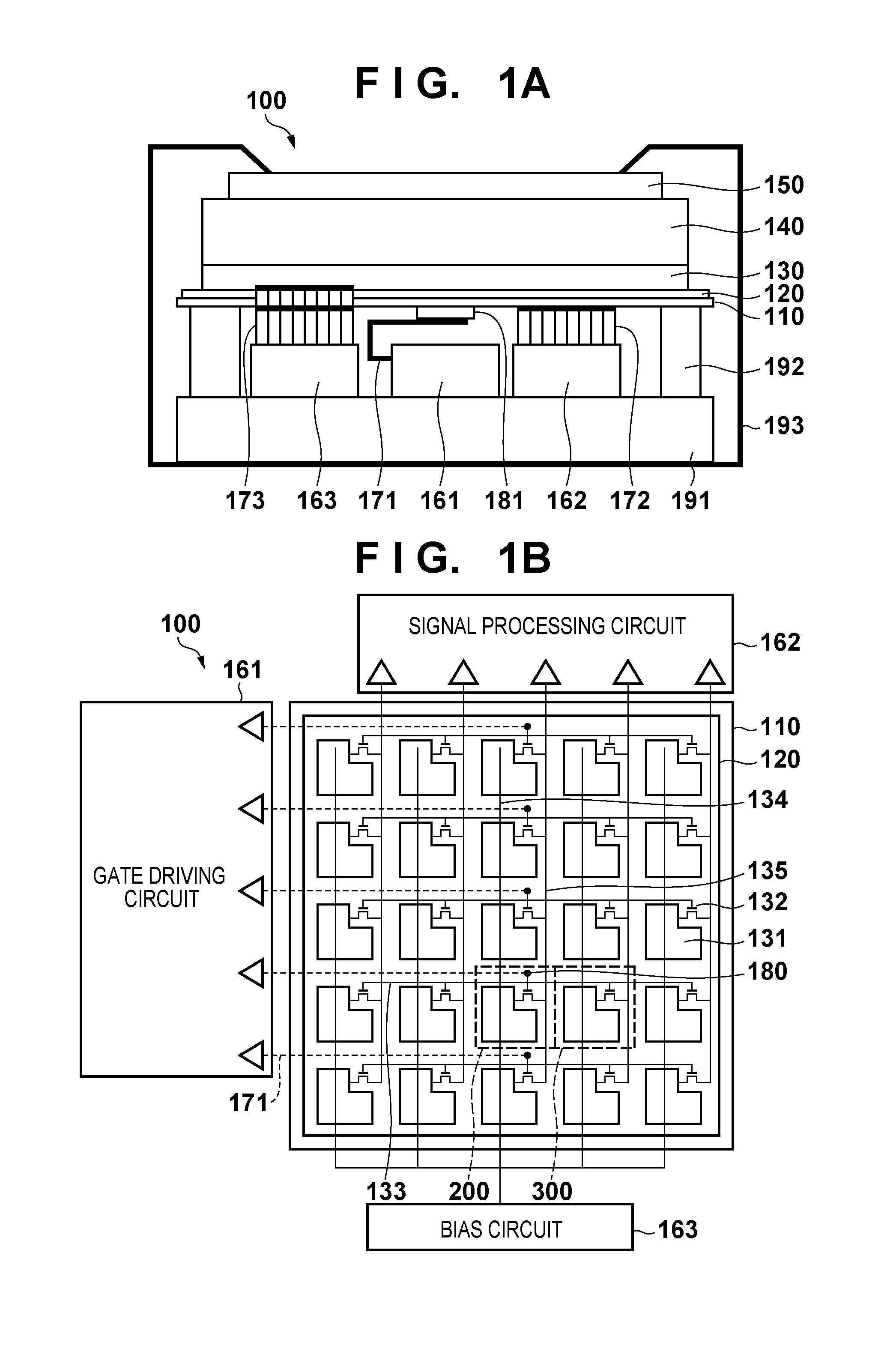
[0021]An example of the entire configuration of a detection apparatus 100 according to the present invention will be described with reference to FIGS. 1A and 1B. FIG. 1A is a front schematic view of the detection apparatus 100, and FIG. 1B is a plan schematic view of the detection apparatus 100. FIG. 1B shows a semiconductor element as an equivalent circuit, and does not illustrate some of components shown in FIG. 1A, for the sake of easy viewing.

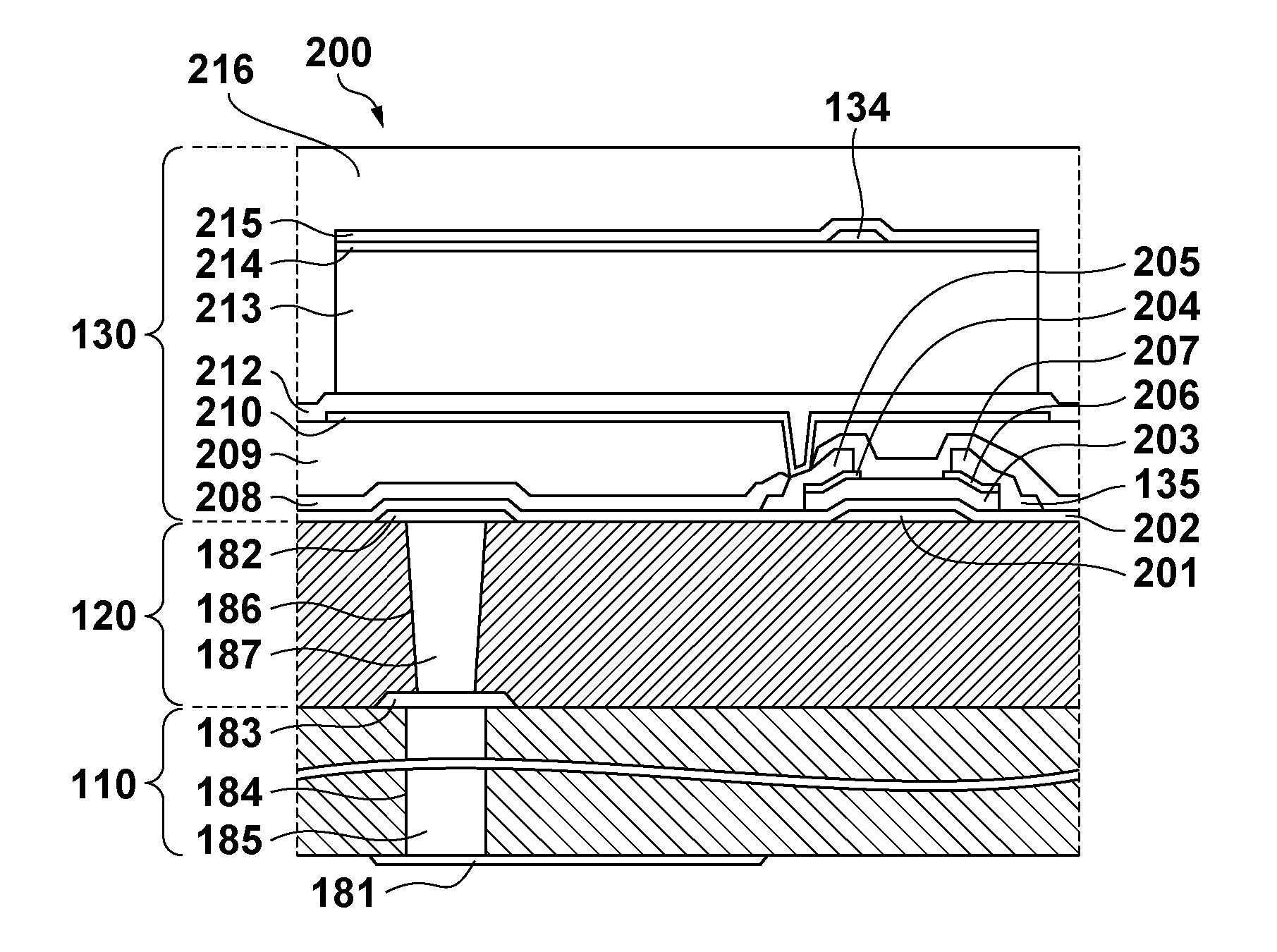
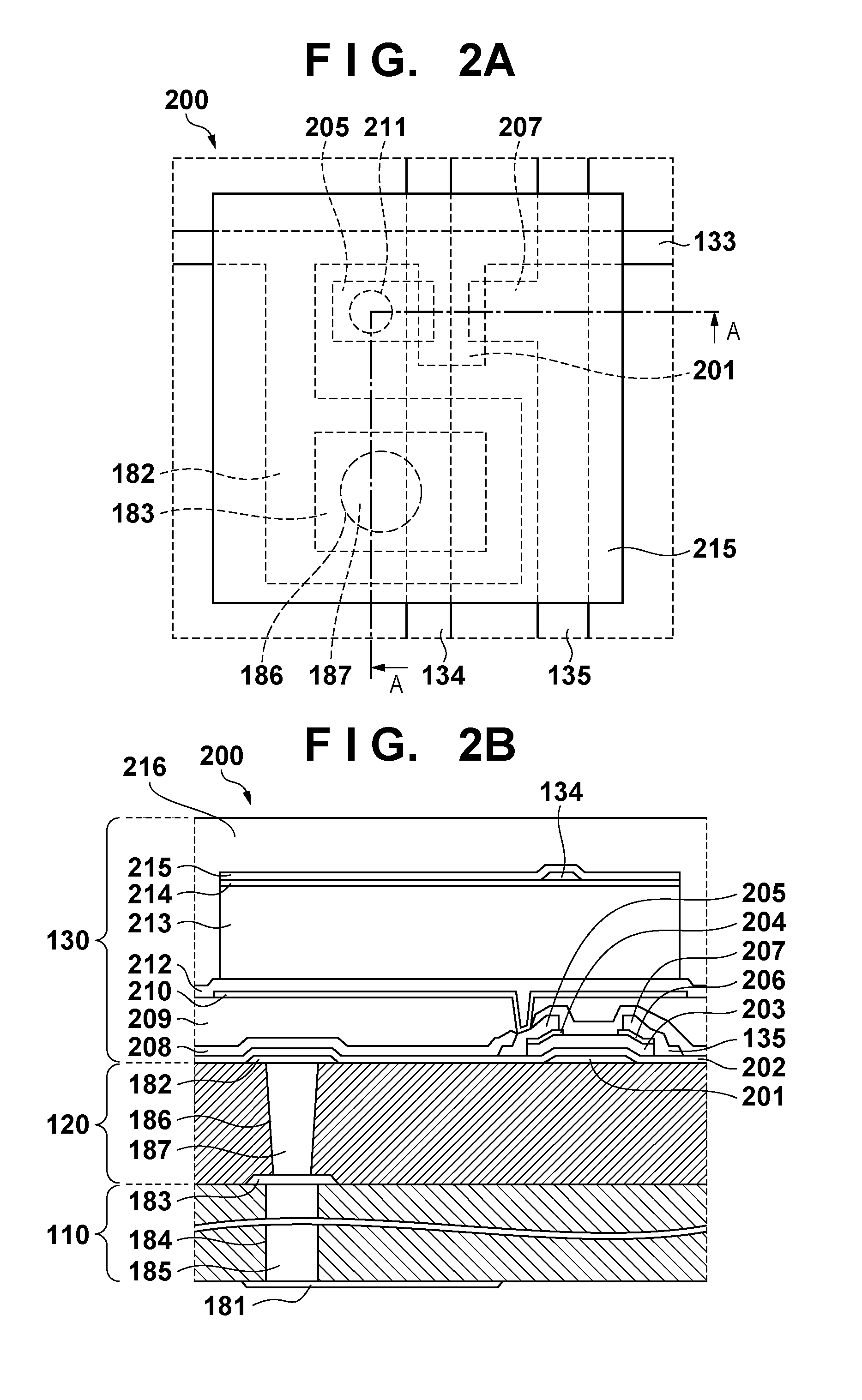
[0022]As shown in FIG. 1A, in the detection apparatus 100, an insulating layer 120 can be arranged on a substrate 110, and a pixel array 130 can be arranged on the insulating layer 120. The substrate 110 can be formed by a material having insulation properties, such as glass or heat-resistant plastic. The insulating layer 120 can be formed by an organic or inorganic material. A scintillator 140 can be arranged on the pixel array 130, and a cover 150 can be arranged on the scintillator 140. The substrate 110 is fixed on a base 191 via a supp...

third embodiment

[0055]Although conductive connection parts are provided mainly on gate lines in the above-mentioned various embodiments, the present invention is also applicable to any conductive line included in a pixel array. For example, a conductive connection part may be provided on the power supply line 904 in the third embodiment, and a voltage may be applied from the central portion of the power supply line 904. This makes it possible to reduce crosstalk generated on the power supply lines 904.


PUM


Abstract

A semiconductor apparatus including a substrate, a pixel array on the substrate, first and second conductive pads between which the substrate locates is provided. The apparatus also comprises an insulating layer arranged between the substrate and the first conductive pad; a third conductive pad arranged between the substrate and the insulating layer; a first conductive member which passes through the insulating layer and connects the first and third conductive pads to each other; and a second conductive member which passes through the substrate and connects the second and third conductive pads to each other. The pixel array further comprises a conductive line connected to circuit elements included in pixels aligned in a row or column direction. The first conductive pad is connected to the conductive line in an interval between the pixels.

Description

BACKGROUND OF THE INVENTION[0001]1. Field of the Invention[0002]The present invention relates to a semiconductor apparatus such as a detection apparatus including a radiation detection apparatus, and a method of manufacturing the same.[0003]2. Description of the Related Art[0004]Japanese Patent Laid-Open No. 2009-133837 proposes a radiation detection apparatus in which an external circuit and a semiconductor element in a pixel array are electrically connected to each other via a conductive adhesive material which penetrates through an insulating layer functioning as a substrate which supports the pixel array. The conductive adhesive material penetrates through the substrate on the outside of the pixel array, and the external circuit is arranged outside the outer periphery of the substrate.SUMMARY OF THE INVENTION[0005]In a semiconductor apparatus such as a detection apparatus including the radiation detection apparatus described in Japanese Patent Laid-Open No. 2009-133837, an exter...

Claims


Application Information

Patent Timeline
Patent Type & Authority Patents(United States)
IPC IPC(8): H01L31/00
CPCH01L27/14603H01L27/14609H01L27/14665H01L27/14683
Inventor WAYAMA, HIROSHIMOCHIZUKI, CHIORIWATANABE, MINORUYOKOYAMA, KEIGOOFUJI, MASATOKAWANABE, JUNFUJIYOSHI, KENTARO
Owner CANON KK
Why Eureka
Try Eureka