Electronic circuit

a technology of electronic circuits and circuits, applied in the direction of power reduction by adiabatic operation, power consumption reduction, pulse technique, etc., can solve problems such as performance degradation of electronic circuits, and achieve the effect of low electrical power voltage and high performan

Active Publication Date: 2013-08-13
SUMITOMO ELECTRIC IND LTD +1
View PDF3 Cites 9 Cited by
  • Summary
  • Abstract
  • Description
  • Claims
  • Application Information

AI Technical Summary

Benefits of technology

[0007]It is an object of the present invention to provide an electronic circuit using low electrical power voltage and having high performance.

Problems solved by technology

However, when the voltage of each stage is reduced, the performance of the electronic circuit may be degraded.

Method used


Image

  • Electronic circuit
  • Electronic circuit
  • Electronic circuit

Examples


first embodiment

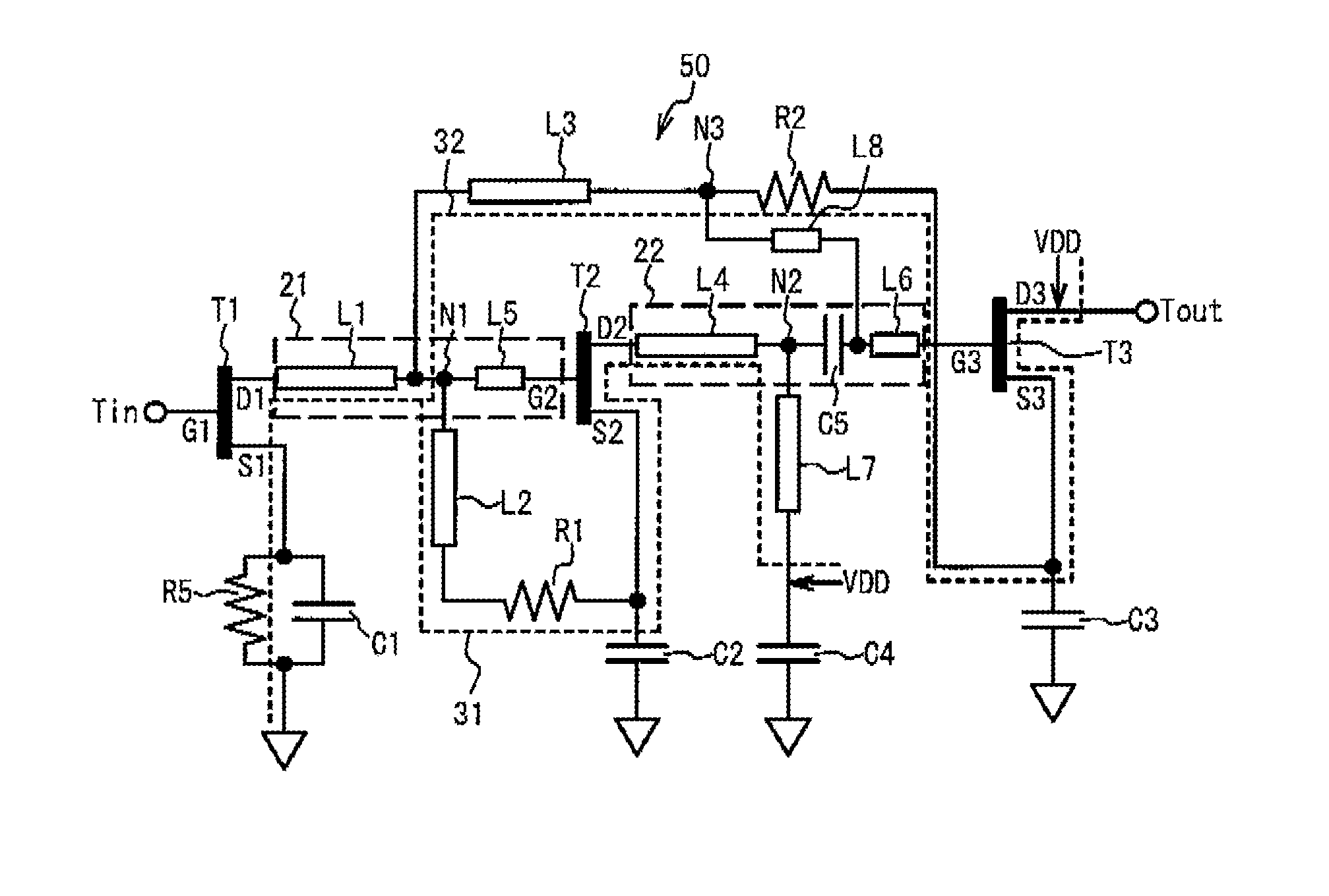
[0031]FIG. 3A illustrates a circuit diagram of an electronic circuit in accordance with a first embodiment. FIG. 3B illustrates a circuit diagram of an electronic circuit in galvanically. In an electronic circuit 50, a distributed parameter line L4, a capacitor C5 and a distributed parameter line L6 are coupled to in series between the drain D2 of the second transistor T2 and the gate G3 of the transistor T3. The node N2 between the distributed parameter line L4 and the capacitor C5 is grounded via the distributed parameter line L7 and the capacitor C4. The direct voltage VDD is applied to a node between the distributed parameter line L7 and the capacitor C4 for cutting direct current via a choke inductor such as a stab. The distributed parameter line L3 and the second resistor R2 are coupled in series between the node N1 and the source S3. A distributed parameter line L8 is coupled between the third node N3 between the distributed parameter line L3 and the second resistor R2 and a ...

second embodiment

[0052]FIG. 5A illustrates a circuit diagram of an electronic circuit in accordance with a second embodiment. FIG. 5B illustrates a circuit diagram of the electronic circuit in galvanically. In an electronic circuit 52, the distributed parameter line L1, the capacitor C6 and the distributed parameter line L5 are coupled in series between the drain D1 of the first transistor T1 and the gate G2 of the second transistor T2. A node between the capacitor C6 and the distributed parameter line L5 is grounded via the resistor R7. The distributed parameter line L3 is coupled between the node N4 between the distributed parameter line L2 and the first resistor R1 and the node N2 between the distributed parameter line L4 and the distributed parameter line L6. In FIG. 5B, the resistor R7 is grounded in galvanically. The distributed parameter lines L1, L2 and L5 and the capacitor C6 make impedance matching between the first transistor T1 and the second transistor T2. The capacitor C6 transmits a h...


PUM


Abstract

An electronic circuit includes: first through third transistors having a control terminal, first and second terminals; a first direct current path supplying a direct current having passed through between the first terminal and the second terminal of at least one of the second transistor and the third transistor to the second terminal of the transistor at former position compared to the transistor through which the direct current passed; a second direct current path that is different from the first direct current path and supplies a direct current having passed through between the first terminal and the second terminal of at least one of the second transistor and the third transistor to the second terminal of the transistor at former position compared to the transistor through which the direct current passed; and a common coupling point coupling the first direct current path and the second direct current path in common.

Description

CROSS-REFERENCE TO RELATED APPLICATION[0001]This application is based upon and claims the benefit of priority of the prior Japanese Patent Application No. 2010-214471, filed on Sep. 24, 2010, the entire contents of which are incorporated herein by reference.BACKGROUND[0002](i) Technical Field[0003]The present invention relates to an electronic circuit, and in particular, relates to a current reuse electronic circuit.[0004](ii) Related Art[0005]There is known a current reuse electronic circuit using a latter DC (direct current) as a former DC in a multiple-stage electronic circuit. Japanese Patent Application Publication No. 2008-35083 (hereinafter referred to as Document 1) discloses an art where a current reuse electronic circuit is used as a doubler.SUMMARY[0006]The current reuse electronic circuit disclosed in Document 1 has a two-stage transistor structure. For example, when the current reuse electronic circuit is structured with three or more stage of transistors in order to im...

Claims


Application Information

Patent Timeline
Patent Type & Authority Patents(United States)
IPC IPC(8): H03F1/26
CPCH03K19/0019
Inventor FUJITA, SEIJITOKUMITSU, TSUNEO
Owner SUMITOMO ELECTRIC IND LTD
Why Eureka
Try Eureka