Solid-state imaging device and control method for same

a technology of solid-state imaging and control method, which is applied in the direction of color television, television system, radio control device, etc., can solve the problems of wasting time, deviating from the time of exposure between the rows on the screen, and worsening the photographic imag

Inactive Publication Date: 2013-08-20
SONY CORP
View PDF23 Cites 9 Cited by
  • Summary
  • Abstract
  • Description
  • Claims
  • Application Information

AI Technical Summary

Problems solved by technology

Differently from the CCD image sensors, because of the use of a focal plane shutter (rolling shutter) to reset the signals on a pixel-row basis by sequentially scanning a multiplicity of pixels arranged two-dimensional, there is a problem that exposure time deviates between the rows on the screen.
(1) In the duration of after a simultaneous transfer over all the rows and before a sequential output on a pixel-row basis, light might leak to the FD the amount of which is different between the rows to be outputted earlier and to be outputted later. This results in a worsened photographic image.
(2) Because the PDs are reset after outputting the information of all the rows, exposure is impossible in a duration from a simultaneous transfer over all the rows to a completion of outputting row by row the information of all the rows. This spends time uselessly. Meanwhile, because of difficulty in taking an exposure time period great, the sensitivity lowers where the subject is dark.
This results in, besides noise or shading, exceeding the amount of saturation signal to cause white skipping in the case of intense light.
In this manner, the leak of light to the FD considerably worsens the photographic image.
Thus, it is impossible to fabricate a structure allowing light to enter only the PD 46.
Thus, the CMOS solid-state imaging device involves a problem that image deterioration is serious upon simultaneous transfer on all the rows.
However, this still requires PD resetting via the FD.
Unless the PD is reset after reading FD signals on all the rows, image deterioration results.
The difference might cause problems, such as fixed-pattern noise and afterimage, not to be removed by the later-processing circuit.
Furthermore, it has been revealed that, in case the PD is reset in a course of FD signal reading by the drain Tr, there encounters a delicate difference between the pixel status before and after resetting the PD thereby causing a problem that a horizontal line is seen in a relevant part of a photographic image.
Meanwhile, it has been also revealed that, in the presence of a drain Tr, there also encounters a problem that a dark current occurs at an oxide film interface in the beneath thereof which flows into the PD.

Method used


Image

  • Solid-state imaging device and control method for same
  • Solid-state imaging device and control method for same
  • Solid-state imaging device and control method for same

Examples


Embodiment Construction

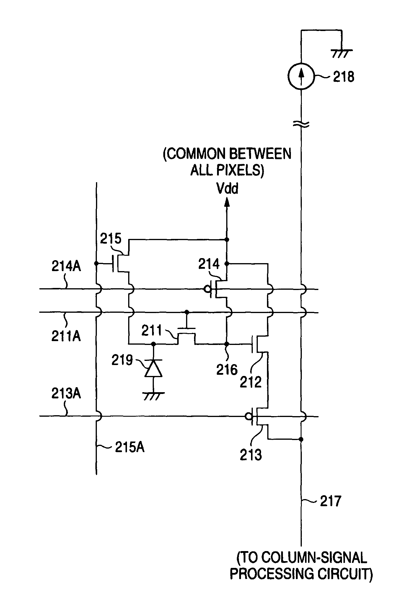
[0052]Now, explanation will be made on the embodiments of a solid-state imaging device, a camera apparatus and a control method for the same according to the invention.

[0053]The present embodiment is of a device structure that a CMOS solid-state imaging device has a drain gate and a transfer gate provided on the respective sides of a PD thereof. The charge stored on the PD can be completely reset / transferred at both the drain and transfer gates, thereby enabling to start a storage in a course of reading a signal of the FD.

[0054]Meanwhile, dark current can be prevented by applying a negative voltage to the drain and transfer gates.

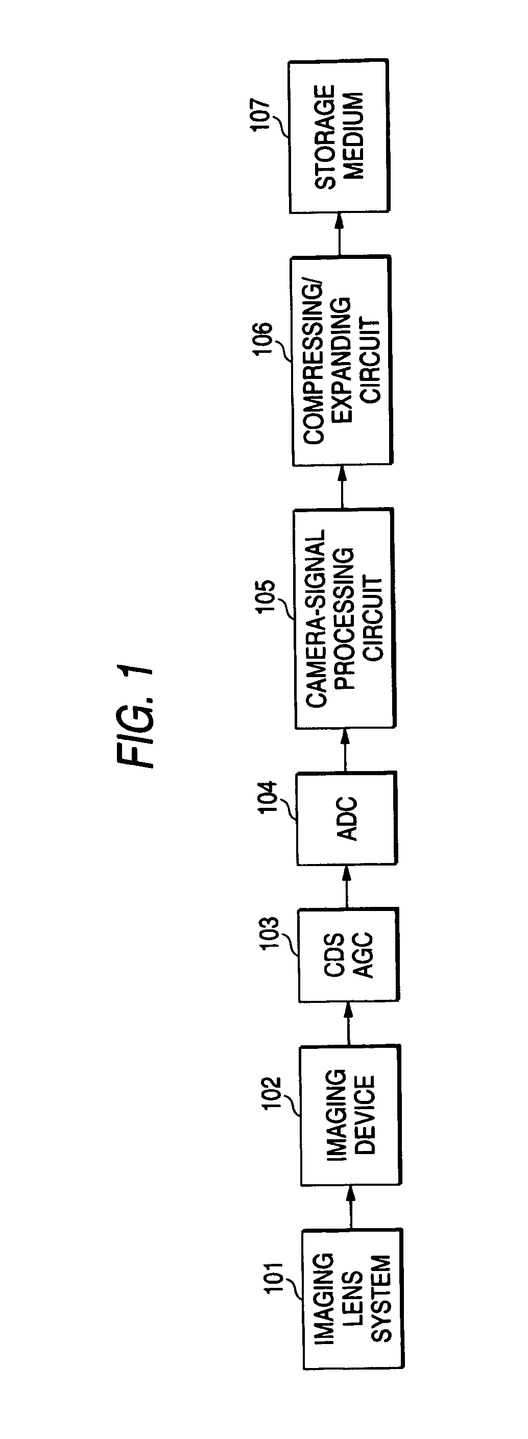
[0055]FIG. 1 is a block diagram showing a configuration example of a camera system according to the embodiment of the present invention.

[0056]The camera system includes an imaging lens system 101, a solid-state imaging device 102, an analog circuit 103, an A / D converter 104, a camera signal processing circuit 105, a compressing / expanding circuit 106 and a s...


PUM


Abstract

In realizing an entire-screen simultaneous shutter function using a solid-state imaging device having a device structure as a CMOS solid-state imaging device, the restriction undergone by exposure time is relieved to secure a sufficient exposure time with swift operation. Separately from a transfer Tr for transferring a signal charge of a buried-type PD to an FD, a drain Tr is provided to exclude a signal charge of the buried PD. Both a channel potential on the drain transistor when turned on and a channel potential on the transfer transistor when turned on are set higher than a depleting potential for the PD. This makes it possible to completely transfer the signal charge of the PD by both the transfer Tr and the drain Tr. In the operation to sequentially read out a signal charge from the FD on a pixel-row basis, PD exposure operation is started in a course of reading out the same.

Description

RELATED APPLICATION DATA[0001]The present application claims priority to Japanese Application(s) No(s). P2002-302873 filed Oct. 17, 2002, which application(s) is / are incorporated herein by reference to the extent permitted by law.BACKGROUND OF THE INVENTION[0002]1. Technical Field of the Invention[0003]The present invention relates to a solid-state imaging device, such as a CMOS image sensor, having an electronic shutter function, and to a control method for same.[0004]2. Description of the Related Art[0005]Conventionally, the CMOS image sensors mostly have electronic shutter functions. Differently from the CCD image sensors, because of the use of a focal plane shutter (rolling shutter) to reset the signals on a pixel-row basis by sequentially scanning a multiplicity of pixels arranged two-dimensional, there is a problem that exposure time deviates between the rows on the screen.[0006]In this case, when shooting a vertically straight object moving in a horizontal direction, it comes...

Claims


Application Information

Patent Timeline
Patent Type & Authority Patents(United States)
IPC IPC(8): H01L27/146H04N1/04H04N5/335H04N5/353H04N5/359H04N5/365H04N5/374
CPCH01L27/14623H01L27/14636H04N5/3532H04N5/359H04N5/374H04N25/531H04N25/62H04N25/76H01L27/146
Inventor MABUCHI, KEIJI
Owner SONY CORP
Why Eureka
Try Eureka