

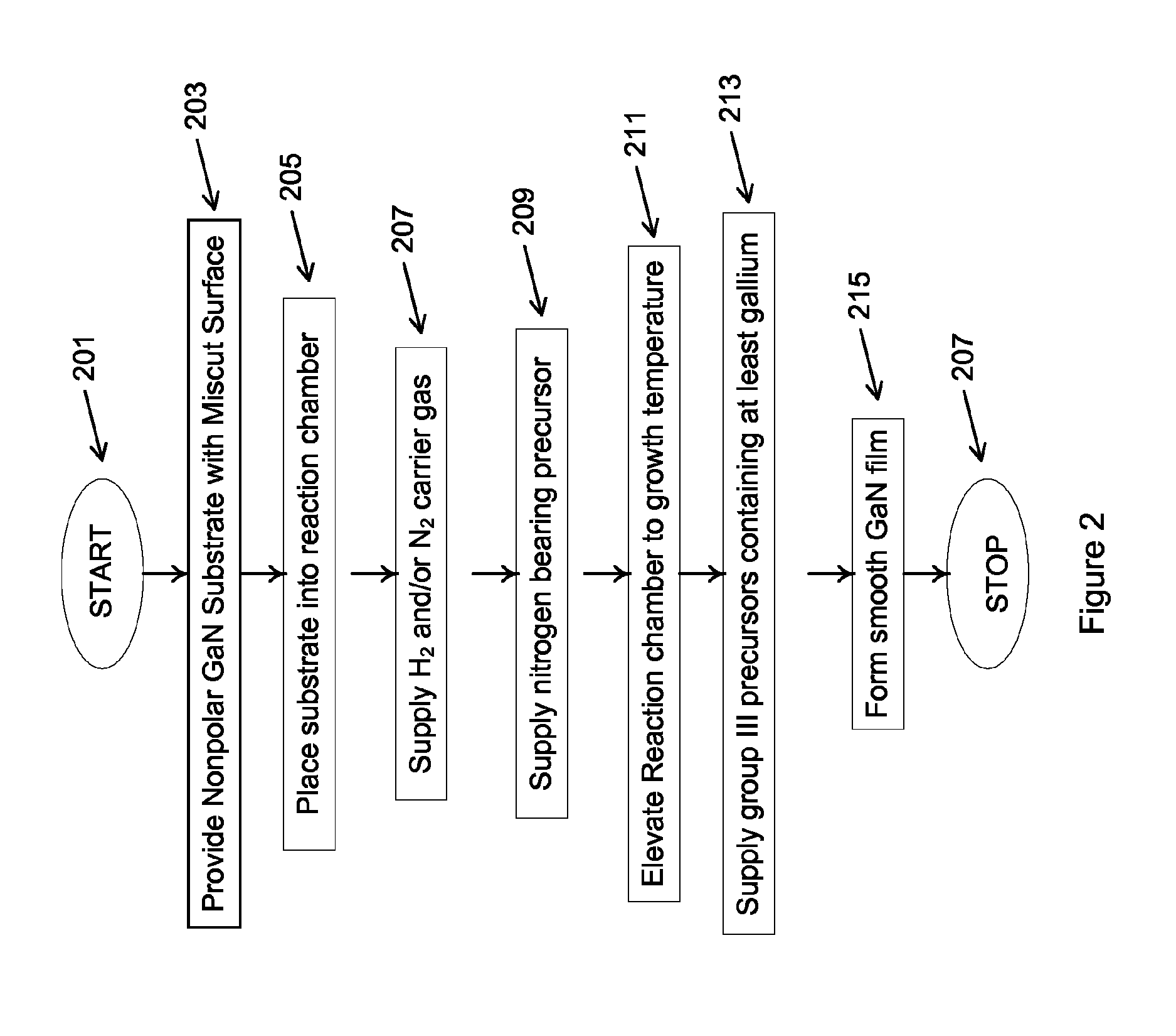
Method and surface morphology of non-polar gallium nitride containing substrates
a gallium nitride and substrate technology, applied in the field of optical devices, can solve the problems of reliability, conventional edison light bulbs dissipate much thermal energy, drawbacks, etc., and achieve the effects of improving device performance, cost-effective manufacturing, and cost-effectiveness
- Summary
- Abstract
- Description
- Claims
- Application Information
AI Technical Summary
Benefits of technology
Problems solved by technology
Method used
Image

Examples
example
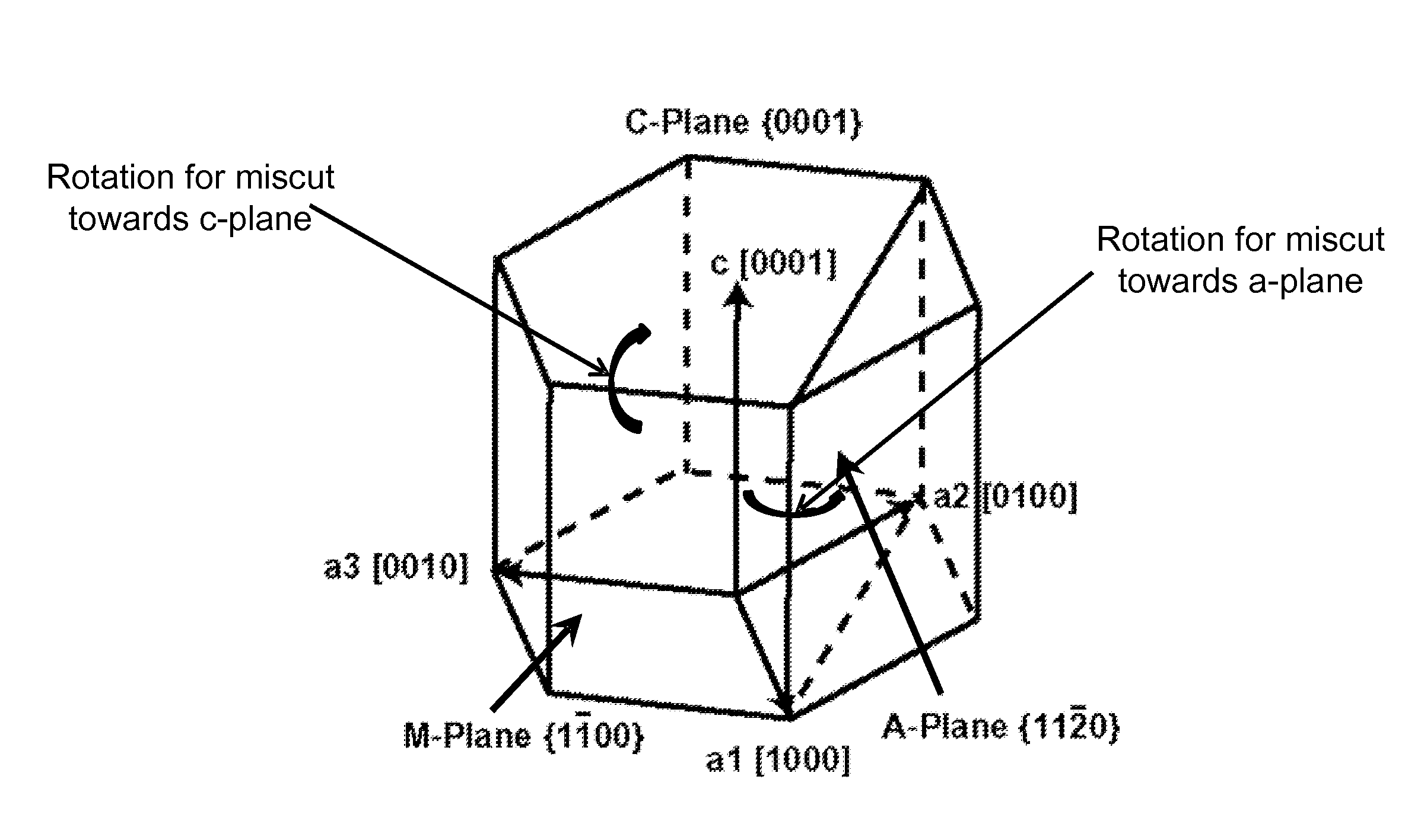
[0084]To prove the operation and method of the present invention, we performed various experiments. These experiments are merely examples, which should not unduly limit the scope of the claims herein. One of ordinary skill in the art would recognize other variations, modifications, and alternatives. As an example, FIG. 4 presents optical micrograph images of the resulting surface morphology in epitaxial films grown with the use of H2 carrier gas on (a) an on-axis nonpolar (10-10) GaN substrate and (b) on a nonpolar (10-10) GaN substrate with a substantial miscut towards the a-plane. FIG. 5 presents images of the resulting surface morphology in epitaxial films grown with the use of H2 carrier gas on nonpolar (10-10) GaN substrates with a varying degree of miscut towards the c-plane. FIG. 6 presents images of the resulting surface morphology in epitaxial films grown on a nominally on-axis nonpolar (10-10) GaN substrate with the use of N2 carrier gas. Further details of our experiments...
PUM
| Property | Measurement | Unit |
|---|---|---|
| atmospheric pressure | aaaaa | aaaaa |
| thickness | aaaaa | aaaaa |
| wavelengths | aaaaa | aaaaa |
Abstract
Description
Claims
Application Information