Horn antenna including integrated electronics and associated method

a technology of integrated electronics and antennas, applied in the field of horn antennas, can solve the problems of high cost, large antennas, and impractical shapes for specific applications, and achieve the effect of low cost and desired bandwidth

Active Publication Date: 2013-10-22
HARRIS CORP
View PDF5 Cites 8 Cited by
  • Summary
  • Abstract
  • Description
  • Claims
  • Application Information

AI Technical Summary

Benefits of technology

[0009]In view of the foregoing background, it is therefore an object of the present invention to provide a horn antenna and associated array which is relatively lightweight, low cost and has desired bandwidth.
[0013]A horn antenna array includes a base PCB, and a plurality of horn antenna devices mounted in an array on the base PCB. Antenna feeds are positioned on a top surface of the base PCB and respectively connected to the wireless communication circuitry of each horn antenna device adjacent a second end thereof opposite the open end of the housing. Array electronic components are positioned on a bottom surface of the base PCB and coupled to the antenna feeds. The base PCB may comprise vias connecting the antenna feeds and the array electronic components. Connection strips may secure edges of the plurality of horn antenna devices together adjacent the first open ends thereof.

Problems solved by technology

These antennas, however, are sometimes large and include impractical shapes for a specific application.
Phased array antennas typically have high size, weight and power (SWaP) and cost issues.
Such high cost limits conventional phased arrays to high end applications.
A typical brick array architecture provides high bandwidth and dense element spacing but is complicated and heavy.

Method used


Image

  • Horn antenna including integrated electronics and associated method
  • Horn antenna including integrated electronics and associated method
  • Horn antenna including integrated electronics and associated method

Examples


Embodiment Construction

[0021]The present invention will now be described more fully hereinafter with reference to the accompanying drawings, in which preferred embodiments of the invention are shown. This invention may, however, be embodied in many different forms and should not be construed as limited to the embodiments set forth herein. Rather, these embodiments are provided so that this disclosure will be thorough and complete, and will fully convey the scope of the invention to those skilled in the art. Like numbers refer to like elements throughout.

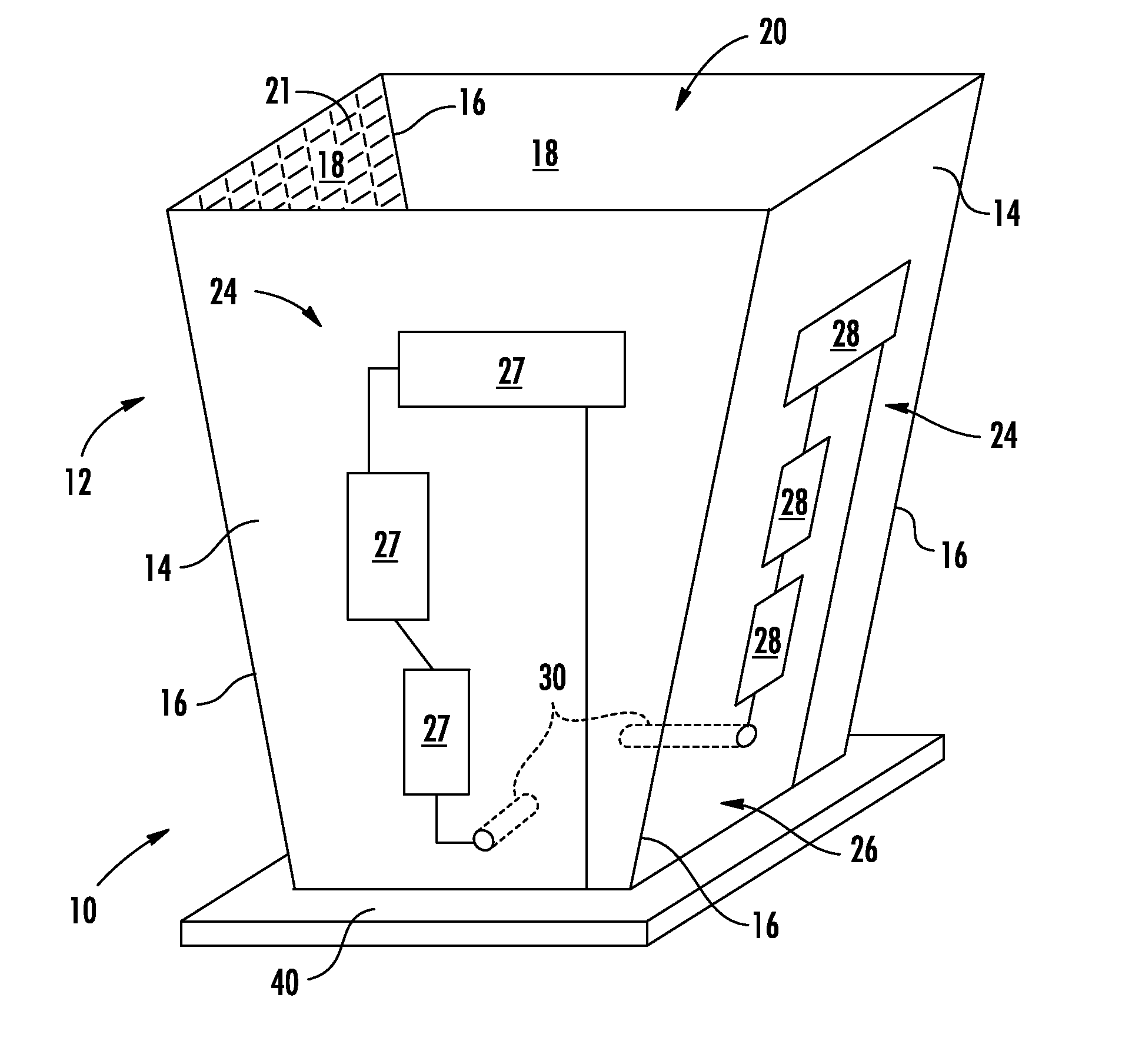
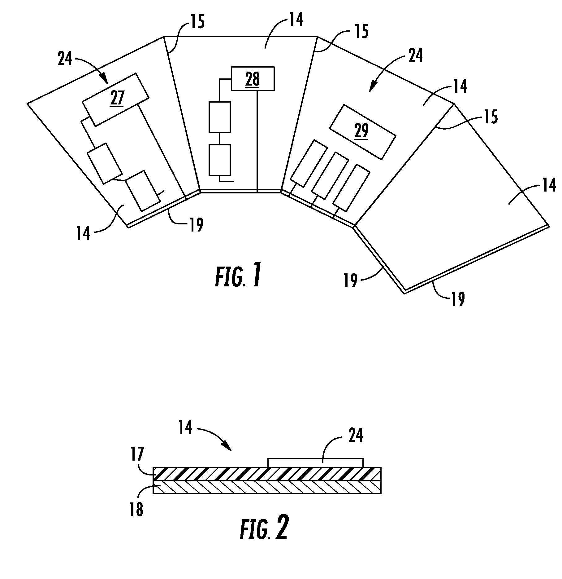
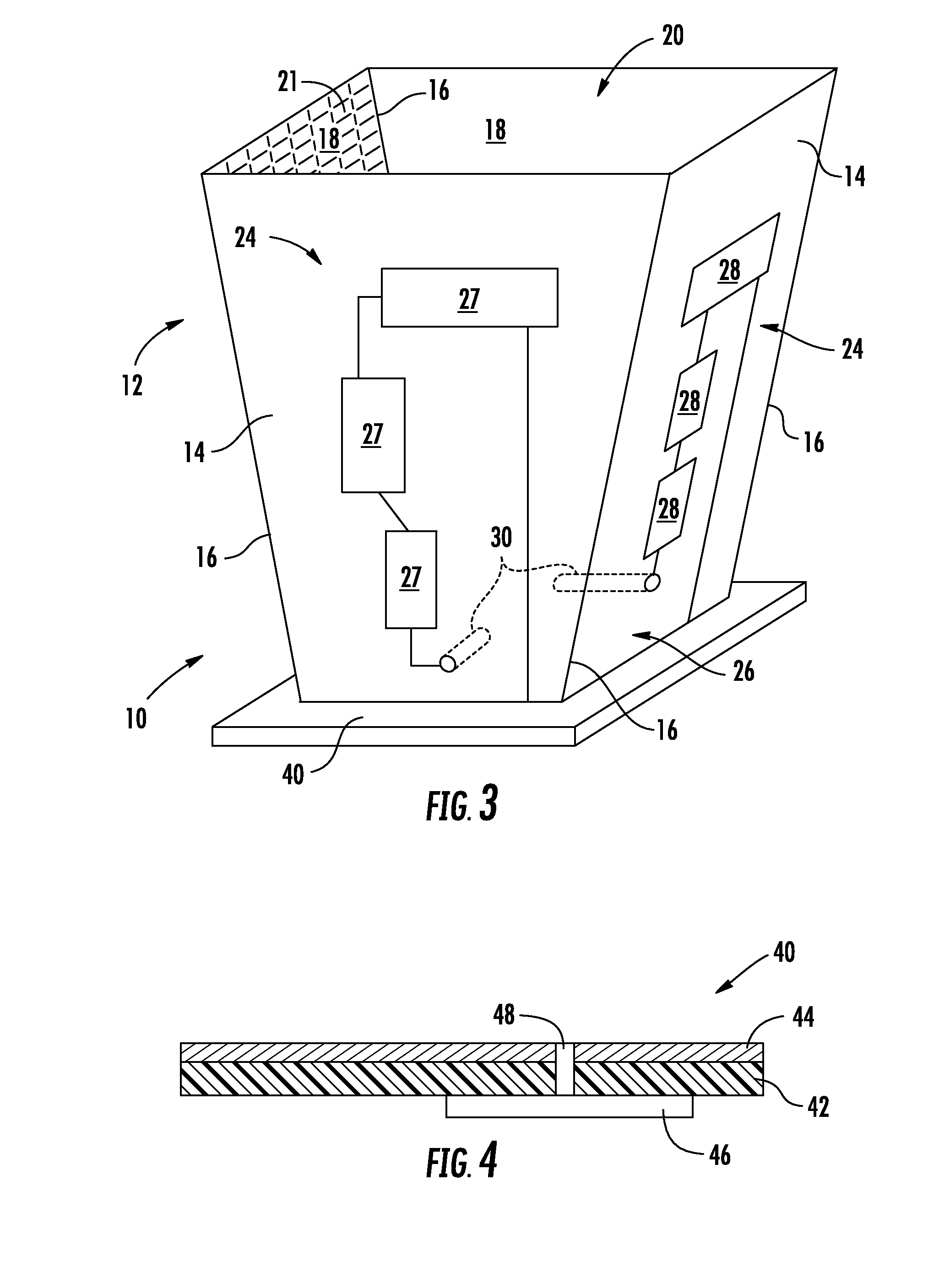
[0022]Referring initially to FIGS. 1-4, a low cost, low weight broadband antenna device 10, e.g. a horn antenna device, and methods of making such devices will now be described. The horn antenna device 10 includes a housing 12 defined by a plurality of printed circuit board (PCB) panels 14 connected together with folded joints or corners 16 therebetween to define a polyhedral shape having a first open end 20. Each of the PCB panels 14 includes a dielectric...


PUM

PropertyMeasurementUnit
shapeaaaaaaaaaa
electrically conductiveaaaaaaaaaa
frequenciesaaaaaaaaaa

Abstract

An antenna device includes a housing having a plurality of printed circuit board (PCB) panels connected together with folded joints therebetween to define a polyhedral shape having a first open end. Each of the PCB panels includes a dielectric substrate and an electrically conductive layer thereon inside of the housing. Wireless communication circuitry is mounted on at least one of the plurality of PCB panels outside the housing, and an antenna feed is connected to the wireless communication circuitry adjacent a second end opposite the first open end of the housing.

Description

FIELD OF THE INVENTION[0001]The present invention relates to the field of antennas, and, more particularly, to horn antennas and horn antenna arrays and related methods.BACKGROUND OF THE INVENTION[0002]In current practice, communications devices are used with many different types of dipoles, biconical dipoles, conical monopoles and discone antennas. These antennas, however, are sometimes large and include impractical shapes for a specific application.[0003]Horn antennas are very popular at UHF (300 MHz-3 GHz) and higher frequencies. They often have a directional radiation pattern with a high gain, which can range up to 25 dB in some cases, with 10-20 dB being typical. Horn antennas have a wide impedance bandwidth. The bandwidth for practical horn antennas can be on the order of 20:1 (e.g. operating from 1 GHz-20 GHz), with a 10:1 bandwidth not being uncommon.[0004]The gain of horn antennas often increases (and the beamwidth decreases) as the frequency of operation is increased. This...

Claims


Application Information

Patent Timeline
Patent Type & Authority Patents(United States)
IPC IPC(8): H01Q13/00
CPCH05K1/0278H01Q21/064H01Q13/02H05K2201/0141H05K2201/047H05K2201/10098H05K2201/0715Y10T29/49018
Inventor MAST, ALAN WILLIAMJANDZIO, GREGORY M.
Owner HARRIS CORP
Why Eureka
Try Eureka