Brick layout and stackup for a touch screen

a touch screen and stacking technology, applied in the field of touch sensor panels, can solve the problem that the touch measurement for a given amount of touch may not be equalized across the touch sensor panel, and achieve the effect of reducing the dynamic range budget, reducing stray capacitance, and reducing calibration difficulty

Active Publication Date: 2013-11-05
APPLE INC
View PDF101 Cites 18 Cited by
  • Summary
  • Abstract
  • Description
  • Claims
  • Application Information

AI Technical Summary

Benefits of technology

[0004]This relates to a touch sensor panel having an array of co-planar single-layer touch sensors fabricated on a single side of a substrate for detecting single or multi-touch events (the touching of one or multiple fingers or other objects upon a touch-sensitive surface at distinct locations at about the same time). The sense (or drive) lines can be fabricated in a single strip as columnar or zig-zag patterns in a first orientation, and the drive (or sense) lines can be fabricated as rows of polygonal (e.g. brick-shaped or pentagonal) conductive areas in a second orientation. Because the drive and sense lines can be formed on the same layer, manufacturing costs can be reduced and the touch sensor panel can be made thinner. Each sense (or drive) line in the first orientation can be coupled to a separate metal trace in the border area of the touch sensor panel, and each polygonal area in the second orientation can also be coupled to a metal trace in the border area of the touch sensor panel. The metal traces in the border areas can be formed on the same side of the substrate as the drive and sense lines. The metal traces can allow both the row and column lines to be routed to the same edge of the substrate so that a small flex circuit can be bonded to a small area on only one side of the substrate.
[0006]Because some bus lines can have much shorter connecting traces to the bricks as compared to other bus lines, the impedance and capacitance of certain bus lines can be much greater than that of other bus lines. Because of this imbalance, touch measurements for a given amount of touch may not be equalized across the touch sensor panel. Therefore, in some embodiments of the invention, the bricks coupled to a particular bus line can be interleaved so that each bus line sees a more uniform average impedance and capacitance, which can help equalize touch measurements across the touch sensor panel.
[0007]Interleaving can additionally provide increased power uniformity. Without interleaving, some drivers can have a small capacitive load, while others can have a large capacitive load. To ensure that the largest load can be properly driven, all drivers may be designed to drive the largest capacitive load, resulting in higher current requirements for all drivers, even those not driven with a large load. However, with interleaving, each driver can have a more moderate and roughly equivalent capacitive load, and the drivers need only be designed to drive the moderate capacitive load.
[0009]For the very longest routing traces, there can be on the order of about 6 pF of Csig transferred from the connecting traces to nearby sense lines, which can reduce the dynamic range budget and can make calibration difficult. Accordingly, a zig-zag double interpolated touch sensor panel can further reduce the stray capacitance between the connecting traces and the sense lines. Polygonal areas representing the drive (or sense) lines generally pentagonal in shape and staggered in orientation can be formed, with some of the polygonal areas near the end of the panel being cut-off pentagons. The sense (or drive) lines are zig-zag shaped. All connecting traces are routed in channels between pentagons. Because the connecting traces do not run alongside any sense (or drive) lines, but instead run between pentagons, the stray capacitance between the connecting traces and the sense (or drive) lines is minimized, and spatial cross-coupling is also minimized.

Problems solved by technology

Because of this imbalance, touch measurements for a given amount of touch may not be equalized across the touch sensor panel.

Method used


Image

  • Brick layout and stackup for a touch screen
  • Brick layout and stackup for a touch screen
  • Brick layout and stackup for a touch screen

Examples


Embodiment Construction

[0025]In the following description of preferred embodiments, reference is made to the accompanying drawings which form a part hereof, and in which it is shown by way of illustration specific embodiments in which the invention can be practiced. It is to be understood that other embodiments can be used and structural changes can be made without departing from the scope of the embodiments of this invention.

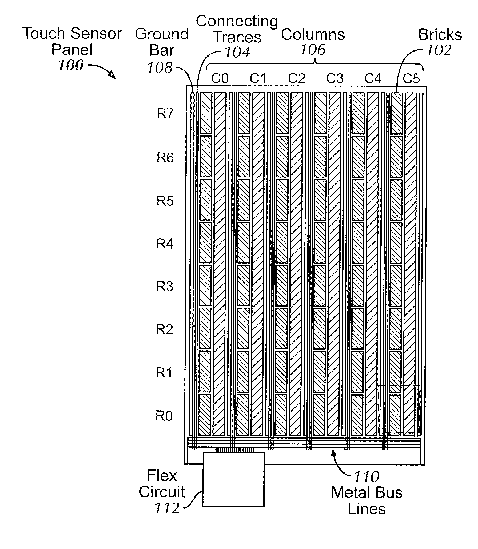
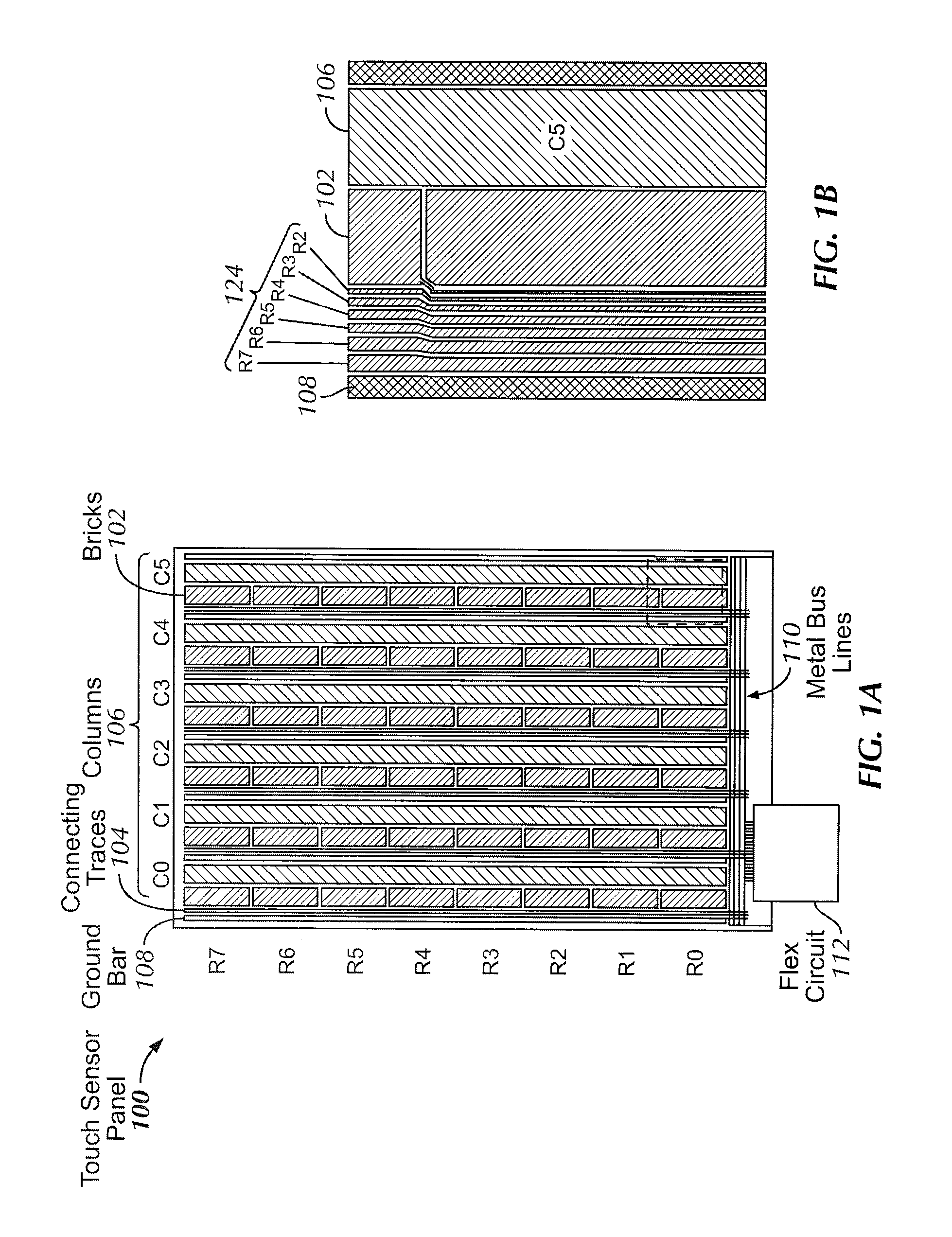
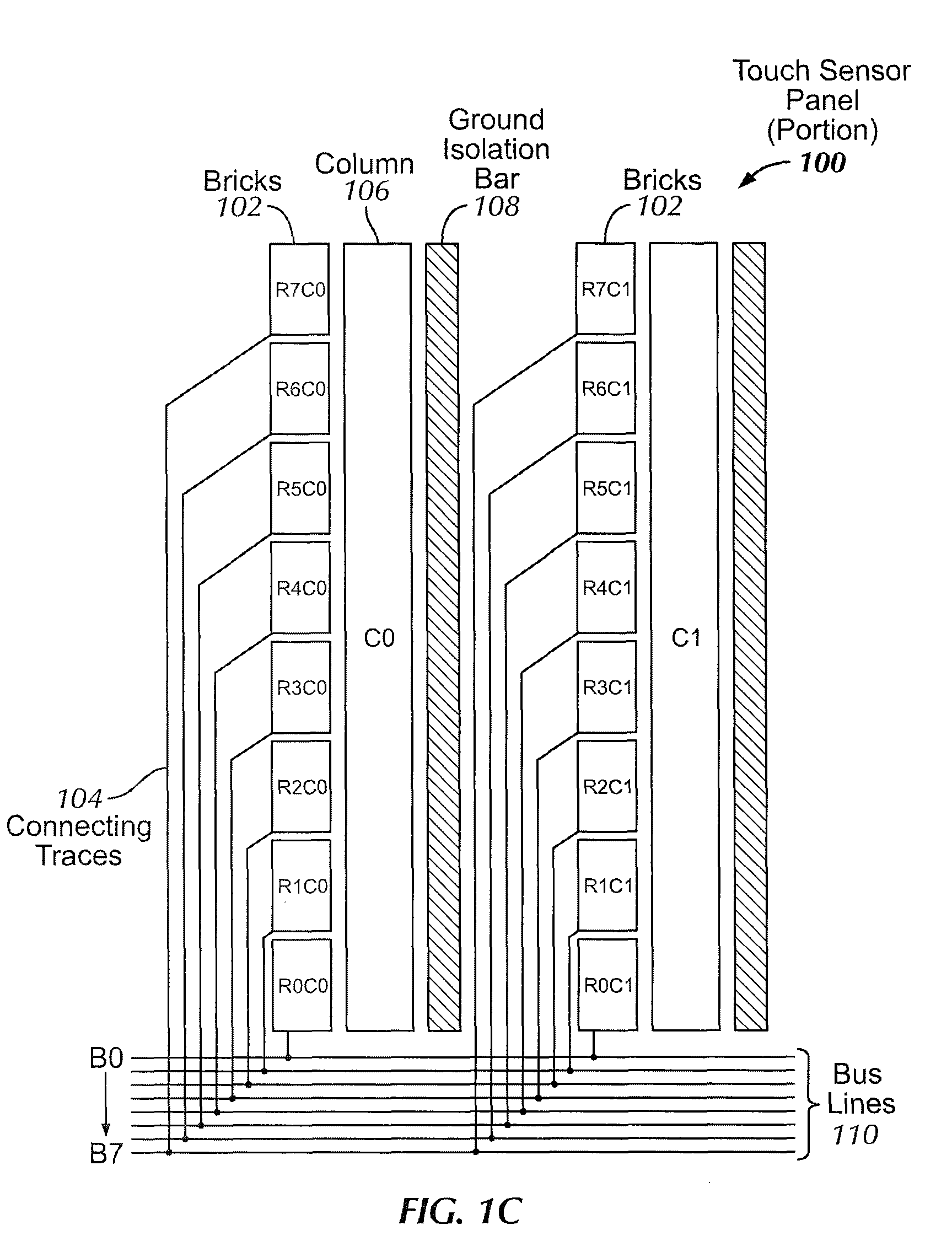
[0026]This relates to a touch sensor panel having an array of co-planar single-layer touch sensors fabricated on a single side of a substrate for detecting single or multi-touch events (the touching of one or multiple fingers or other objects upon a touch-sensitive surface at distinct locations at about the same time). In mutual capacitance embodiments, each sensor or pixel can be the result of interactions between drive and sense lines. The sense (or drive) lines can be fabricated in a single strip as columnar or zig-zag patterns in a first orientation, and the drive (or sense) line...


PUM


Abstract

A touch sensor panel is disclosed having an array of co-planar single-layer touch sensors fabricated on a single side of a substrate. The sense (or drive) lines can be fabricated in a single strip as columnar or zig-zag patterns in a first orientation, and the drive (or sense) lines can be fabricated as rows of polygonal (e.g. brick-shaped or pentagonal) conductive areas in a second orientation. Each sense (or drive) line in the first orientation can be coupled to a separate metal trace in the border area of the touch sensor panel, and each polygonal area in the second orientation can also be coupled to a metal trace in the border area of the touch sensor panel. The metal traces can allow both the row and column lines to be routed to the same edge of the substrate for flex circuit attachment.

Description

FIELD OF THE INVENTION[0001]This relates generally to input devices for computing systems, and more particularly, to a touch sensor panel capable of being fabricated on a single side of a substrate.BACKGROUND OF THE INVENTION[0002]Many types of input devices are presently available for performing operations in a computing system, such as buttons or keys, mice, trackballs, touch sensor panels, joysticks, touch screens and the like. Touch screens, in particular, are becoming increasingly popular because of their ease and versatility of operation as well as their declining price. Touch screens can include a touch sensor panel, which can be a clear panel with a touch-sensitive surface. The touch sensor panel can be positioned in front of a display screen so that the touch-sensitive surface covers the viewable area of the display screen. Touch screens can allow a user to make selections and move a cursor by simply touching the display screen via a finger or stylus. In general, the touch ...

Claims


Application Information

Patent Timeline
Patent Type & Authority Patents(United States)
IPC IPC(8): G06F3/045
CPCG06F3/0416G06F3/044G06F2203/04107G06F3/0443
Inventor HOTELLING, STEVE PORTER
Owner APPLE INC
Why Eureka
Try Eureka