Digitally controlled antenna tuning circuit for radio frequency receivers

a digital control and antenna technology, applied in the direction of antennas, electrically long antennas, electrically short antennas, etc., can solve the problems of limited dynamic range of circuits, limited bandwidth defined by the impedance matching network, and relatively expensive components of commonly used pin diodes, etc., to achieve the effect of low cos

Inactive Publication Date: 2013-11-12
VISHAY INTERTECHNOLOGY INC
View PDF51 Cites 12 Cited by
  • Summary
  • Abstract
  • Description
  • Claims
  • Application Information

AI Technical Summary

Benefits of technology

[0035]The present invention is a novel digitally controlled antenna tuning circuit that overcomes the disadvantages and drawbacks of prior art tuning circuits. The antenna tuning circuit of the present invention enables the implementation of low cost, wideband tuning circuits for antennas in receive applications.
[0039]The use of the antenna tuning circuits of the present invention provides numerous advantages, including the following: (1) the ability to reduce the number of PIN diodes required per tuning element from two or four in prior art circuits to one, thus significantly reducing the cost of the resulting circuit; (2) the ability to configure tuning elements in the antenna tuning circuit in either a parallel or series configuration; and (3) the ability to use any combination and number of capacitors and inductors in the antenna tuning circuit in any desired parallel or series configuration.

Problems solved by technology

Often times, however, the natural operating frequency band of the antenna is either (1) not sufficiently wide enough to cover the needs of the wireless system or (2) is not in the proper spectrum location where the antenna is required to function.
By definition, however, the impedance matching network has a limited defined bandwidth.
Regarding the varactor based tuning circuits described above, the use of varactors limits the dynamic range of the circuit.
Commonly used PIN diodes are relatively expensive components.
Thus, a disadvantage of this topology is the large number of PIN diodes required to realize the circuit.
Such high powered signals are likely to affect the DC bias point of the PIN diodes.

Method used


Image

  • Digitally controlled antenna tuning circuit for radio frequency receivers
  • Digitally controlled antenna tuning circuit for radio frequency receivers
  • Digitally controlled antenna tuning circuit for radio frequency receivers

Examples


first embodiment

Antenna Tuning Circuit

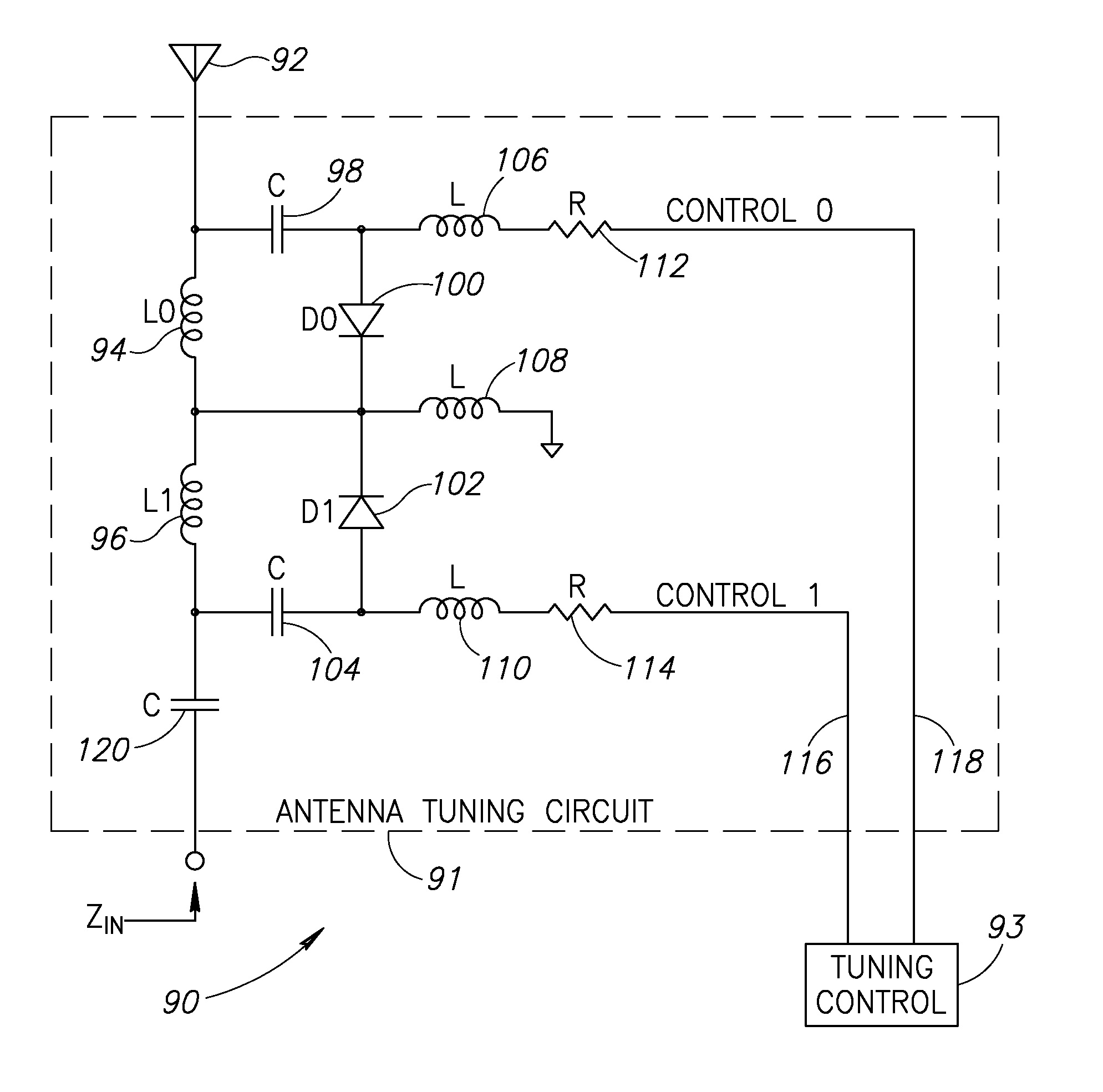
[0069]A schematic diagram illustrating a first example embodiment of the antenna tuning circuit of the present invention having series connected tuning elements is shown in FIG. 5. The circuit, generally referenced 90, comprises a tuning circuit 91 coupled to antenna 92 and a tuning control circuit 93. The tuning circuit comprises two series connected tuning stages comprising tuning elements made up of inductors L0 (94), L1 (96), DC blocking capacitors C 98, 104, 120, RF chokes L 106, 108, 110, resistors R 112, 114 and switching devices comprising PIN diodes D0 (100), D1 (102).

[0070]In accordance with the invention, it is assumed that the signals flowing through the main receive signal path are sufficiently weak enough to allow the use of a single PIN diode to short circuit a single tuning stage. In the example circuit 90, the main receive signal path comprises two tuning elements connected in series (L0 and L1).

[0071]Two switching elements comprising PIN diode...

second embodiment

Antenna Tuning Circuit

[0077]A schematic diagram illustrating a second example embodiment of the antenna tuning circuit of the present invention having series connected tuning elements is shown in FIG. 6. The circuit, generally referenced 220, comprises a tuning circuit 221 coupled to antenna 222 and a tuning control circuit 223. The tuning circuit comprises four series connected tuning stages comprising tuning elements made up of inductors L0 (224), L1 (226), L2 (228), L3 (230), DC blocking capacitors C 232, 242, 246, 252, 256, 266, RF chokes L 236, 240, 260, 258, 268, resistors R 238, 250, 262, 270 and switching devices comprising PIN diodes D0 (234), D1 (244), D2 (254), D3 (264).

[0078]In this example circuit 221, four tuning stages comprising tuning elements L0, L1, L2 and L3 are connected in series to form the main receive signal path. Corresponding PIN diodes D0, D1, D2 and D3, connected in parallel to the tuning elements, act as switches to switch each respective tuning element...

third embodiment

Antenna Tuning Circuit

[0079]A schematic diagram illustrating a third example embodiment of the antenna tuning circuit of the present invention having series connected tuning elements is shown in FIG. 7. The circuit, generally referenced 130, comprises a tuning circuit 131 coupled to antenna 132 and a tuning control circuit 133. The tuning circuit comprises two series connected tuning stages comprising tuning elements made up of capacitors C0 (134), C1 (136), DC blocking capacitor C 138, RF chokes L 144, 148, 150, resistors R 146, 152 and switching devices comprising PIN diodes D0 (140), D1 (142).

[0080]In this example circuit 131, two tuning stages comprising tuning elements capacitors C0 and C1 are connected in series to form the main receive signal path rather than inductors as in the example circuits 91 (FIG. 5) and 221 (FIG. 6). Corresponding PIN diodes D0 and D1 connected in parallel to the tuning elements act as switches to switch each respective tuning element either into or o...


PUM


Abstract

A novel digitally controlled antenna tuning circuit that enables the implementation of low cost, wideband tuning circuits for antennas in receive applications. The invention is operative to switch a plurality of tuning elements into and out of a main receive signal path. Each individual tuning element is switched into or out of the receive signal path using a single PIN diode. For series connected tuning elements, the diode is connected in parallel to the tuning element. For tuning elements connected in parallel, the diode is connected in series with the tuning element. The diodes are switched in accordance with control voltages which forward bias the diodes to effectively create a low resistance path thus either inserting or removing a tuning element from the receive signal path depending on its configuration in the circuit.

Description

FIELD OF THE INVENTION[0001]The present invention relates generally to antenna tuning circuits and more particularly to digitally controlled antenna tuning circuits for use with radio frequency (RF) receivers.BACKGROUND OF THE INVENTION[0002]As the use of computers and especially handheld or mobile electronic devices continues to increase at a rapid rate, the demand for peripherals and systems connected via wireless connections continues to increase. The number of wireless applications is currently increasing at a very high rate in areas such as security alarms, networking, personal computing, data communications, telephony and computer security.[0003]Wireless communications currently may take many forms such as ultrasonic, IR and RF. In the case of RF communications, wireless transmitters, receivers and transceivers use one or more antenna elements to convert an electrical RF signal to and from an electromagnetic wave. During transmission, the antenna serves as a radiator, generati...

Claims


Application Information

Patent Timeline
Patent Type & Authority Patents(United States)
IPC IPC(8): H04B1/26
CPCH04B1/18H01Q1/24H04B1/40H01Q9/00
Inventor BEN-BASSAT, DAVID
Owner VISHAY INTERTECHNOLOGY INC
Why Eureka
Try Eureka