Liquid crystal display device and television set

a technology of liquid crystal display and television set, which is applied in the direction of display means, semiconductor devices, instruments, etc., can solve the problems of increasing heat generation inevitably, and achieve the effect of avoiding heat concentration

Active Publication Date: 2013-12-03
PANASONIC INTELLECTUAL PROPERTY CORP OF AMERICA +1
View PDF28 Cites 5 Cited by
  • Summary
  • Abstract
  • Description
  • Claims
  • Application Information

AI Technical Summary

Benefits of technology

[0009](1) A liquid crystal display device according to the present invention includes: a liquid crystal display panel; and a backlight unit, in which: the backlight unit includes: a plurality of light emitting diodes each having an anode and a cathode; a first substrate; and a second substrate, the plurality of light emitting diodes being mounted on the first substrate and the second substrate; the first substrate and the second substrate are disposed adjacent to each other; light emitting diodes, which are adjacent across a boundary between the first substrate and the second substrate, of the plurality of light emitting diodes are disposed so that the respective anodes are opposed to each other and so as to have a pitch equal to or smaller than a pitch of other adjacent light emitting diodes of the plurality of light emitting diodes. According to the present invention, a pair of the light emitting diodes having a small pitch are disposed so that respective anodes are opposed to each other. Therefore, the respective cathodes, at which heat is easily generated, are kept away from each other, and hence it is possible to avoid heat concentration.

Problems solved by technology

In such a case, heat generation inevitably increases at a portion where the light emitting diodes are provided close to one another.

Method used


Image

  • Liquid crystal display device and television set
  • Liquid crystal display device and television set
  • Liquid crystal display device and television set

Examples


first embodiment

[Modified Example of First Embodiment]

[0069]FIG. 6 is a wiring diagram of the first substrate 18-1 and the second substrate 18-2 of a liquid crystal display device according to a modified example of the first embodiment of the present invention.

[0070]In this modified example, first anode wiring 142 and second anode wiring 146 are each wired on an outer side of the light emitting diodes 16 connected in series in two rows. Specifically, the plurality of light emitting diodes 16 are respectively arranged on the first substrate 18-1 and the second substrate 18-2 in a plurality of rows. The first anode wiring 142 is disposed so as to pass one of regions opposing across all of the light emitting diodes 16 arranged in the plurality of rows on the first substrate 18-1. The second anode wiring 146 is disposed so as to pass one of regions opposing across all of the light emitting diodes 16 arranged in the plurality of rows on the second substrate 18-2. The first anode wiring 142 and the secon...

second embodiment

[Second Embodiment]

[0071]FIG. 7 is a wiring diagram of the first substrate 18-1 and the second substrate 18-2 of a liquid crystal display device according to a second embodiment of the present invention.

[0072]In this embodiment, the light emitting diodes 16 on the first substrate 18-1 are arranged in one row. The light emitting diodes 16 on the second substrate 18-2 are also arranged in one row. Other contents correspond to the contents described in the above-mentioned first embodiment.

[Third Embodiment]

[0073]FIG. 8 is a wiring diagram of the first substrate 18-1 and the second substrate 18-2 of a liquid crystal display device according to a third embodiment of the present invention.

[0074]A connector 19 is mounted on the first substrate 18-1. The connector 19 is mounted at an end portion of the first substrate 18-1 on a side opposite to the second substrate 18-2. Meanwhile, a connector is not mounted on the second substrate 18-2. That is, electrical connection with the inverter (not...

third embodiment

[Modified Example of Third Embodiment]

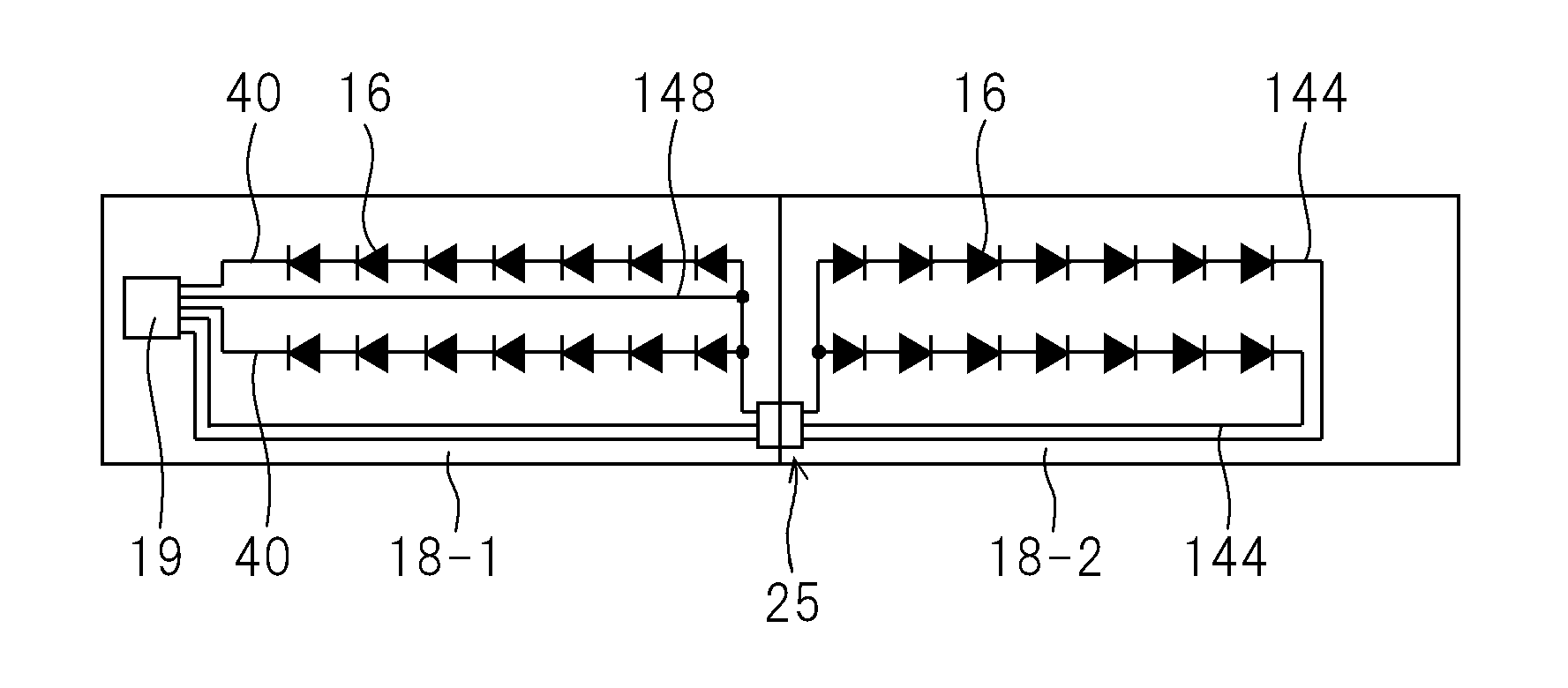
[0080]FIG. 9 is a wiring diagram of the first substrate 18-1 and the second substrate 18-2 of a liquid crystal display device according to a modified example of the third embodiment of the present invention.

[0081]In this modified example, anode wiring 148 is disposed so as to pass between the light emitting diodes 16 arranged in the plurality of rows on the first substrate 18-1, which is different from the above-mentioned third embodiment. Other contents correspond to the contents described in the above-mentioned third embodiment. For example, also in this modified example, the plurality of light emitting diodes 16 are respectively arranged on the first substrate 18-1 and the second substrate 18-2 in a plurality of rows. Further, the second cathode wiring 144 is disposed so as to pass one of regions opposing across all of the light emitting diodes 16 arranged in the plurality of rows on the first substrate 18-1 and the second substrate 18-2.

[008...


PUM


Abstract

Provided is a liquid crystal display device, including: a liquid crystal display panel; and a backlight unit, in which: the backlight unit includes: a plurality of light emitting diodes each having an anode and a cathode; a first substrate; and a second substrate, the plurality of light emitting diodes being mounted on the first substrate and the second substrate; the first substrate and the second substrate are disposed adjacent to each other; light emitting diodes which are adjacent across a boundary between the first substrate and the second substrate are disposed so that the respective anodes are opposed to each other and so as to have a pitch equal to or smaller than a pitch of other adjacent light emitting diodes.

Description

CROSS-REFERENCE TO RELATED APPLICATION[0001]The present application claims priority from Japanese application JP 2010-146547 filed on Jun. 28, 2010, the content of which is hereby incorporated by reference into this application.BACKGROUND OF THE INVENTION[0002]1. Field of the Invention[0003]The present invention relates to a liquid crystal display device.[0004]2. Description of the Related Art[0005]Light emitting diodes (LEDs) have become widely used as light sources of a backlight unit. For example, there is known an edge light type backlight unit in which, instead of cold-cathode tubes, light emitting diodes are disposed on an end surface of a light guide plate so as to enable surface emission by the light guide plate. Further, there is known an example using light emitting diodes in a direct type backlight unit (Japanese Patent Application Laid-open No. 2009-87879).[0006]In a conventional direct type or edge type backlight unit, the light emitting diodes are generally arranged ev...

Claims


Application Information

Patent Timeline
Patent Type & Authority Patents(United States)
IPC IPC(8): H01L33/08
CPCG02F1/133603G02F2001/133628G02F2001/133612G02F1/133612G02F1/133628
Inventor BABA, MASASHIIMAJO, IKUKOMATSUDA, ISAO
Owner PANASONIC INTELLECTUAL PROPERTY CORP OF AMERICA
Why Eureka
Try Eureka