Semiconductor device

a technology of semiconductor devices and semiconductors, applied in semiconductor devices, solid-state devices, basic electric elements, etc., can solve problems such as difficulty in developing semiconductor device characteristics

Active Publication Date: 2022-09-27
FUJI ELECTRIC CO LTD
View PDF17 Cites 0 Cited by
  • Summary
  • Abstract
  • Description
  • Claims
  • Application Information

AI Technical Summary

Benefits of technology

[0057]According to the disclosed technique, heat concentration is prevented and the characteristics of the semiconductor device are improved.

Problems solved by technology

However, heat generated is concentrated at the central portion (one portion) of the substrate over which the IGBTs and FWDs are intensively disposed.
As a result, the rated current and the like of a semiconductor device are influenced and it may be difficult to develop the characteristics of the semiconductor device.

Method used


Image

  • Semiconductor device
  • Semiconductor device
  • Semiconductor device

Examples


first embodiment

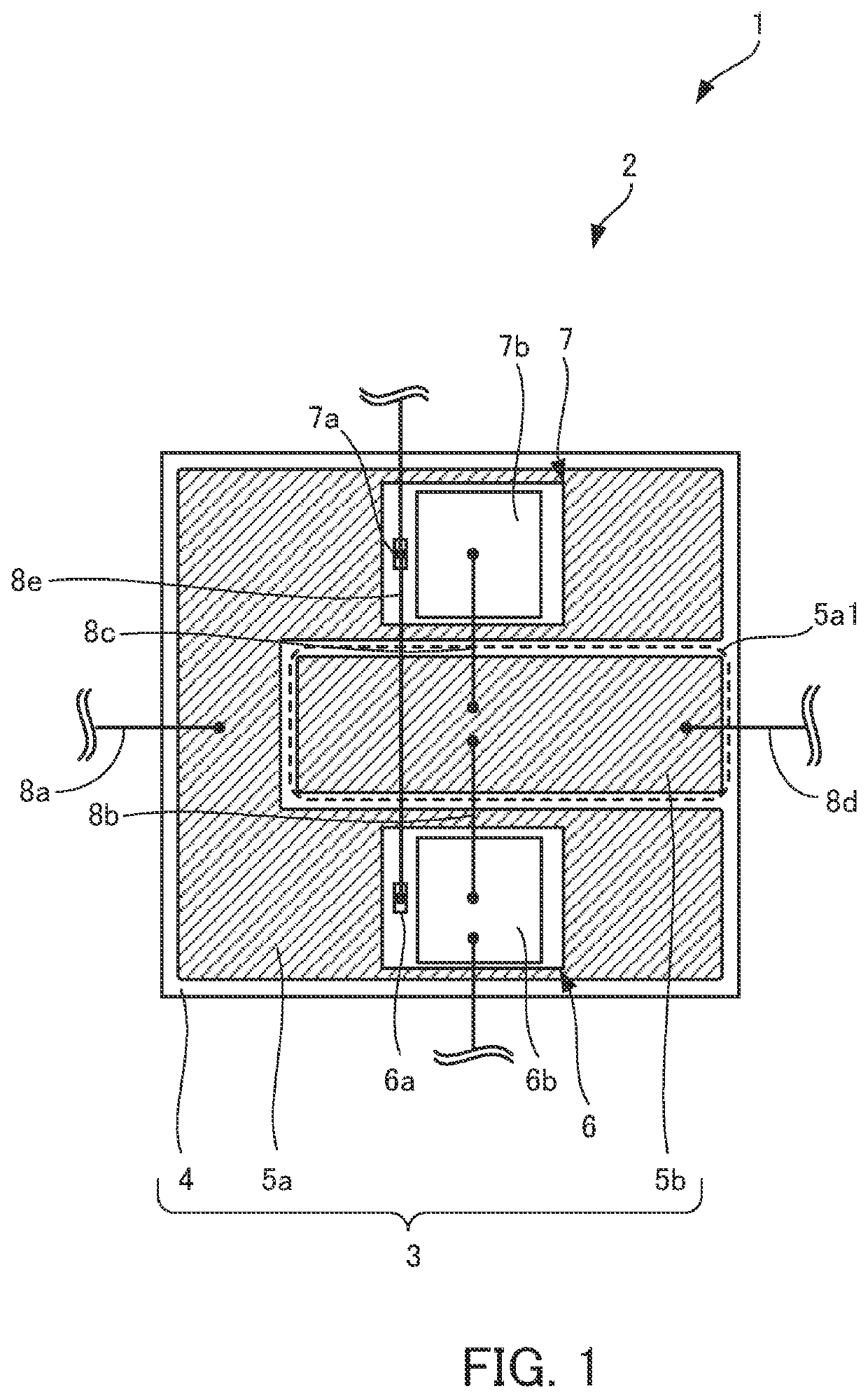
[0015]An arm block included in a semiconductor device according to a first embodiment will now be described by the use of FIG. 1. FIG. 1 is a view for describing an arm block included in a semiconductor device according to a first embodiment. A semiconductor device 1 according to a first embodiment includes an arm block 2 illustrated in FIG. 1. The arm block 2 includes a laminated substrate 3 and first semiconductor chips 6 and disposed over the laminated substrate 3. The first semiconductor chip 6 has a first positive electrode (not illustrated) on the back surface and has a first negative electrode 6b and a first control electrode 6a on the front surface. The first semiconductor chip 7 has a first positive electrode (not illustrated) on the back surface and has a first negative electrode 7b and a first control electrode 7a on the front surface. The first semiconductor chips 6 and 7 may be, for example, power MOSFETs or reverse-conducting (RC)-IGBTs. With the RC-IGBTs an IGBT and a...

second embodiment

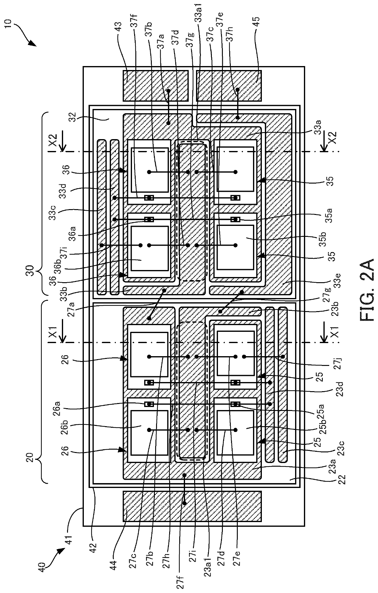
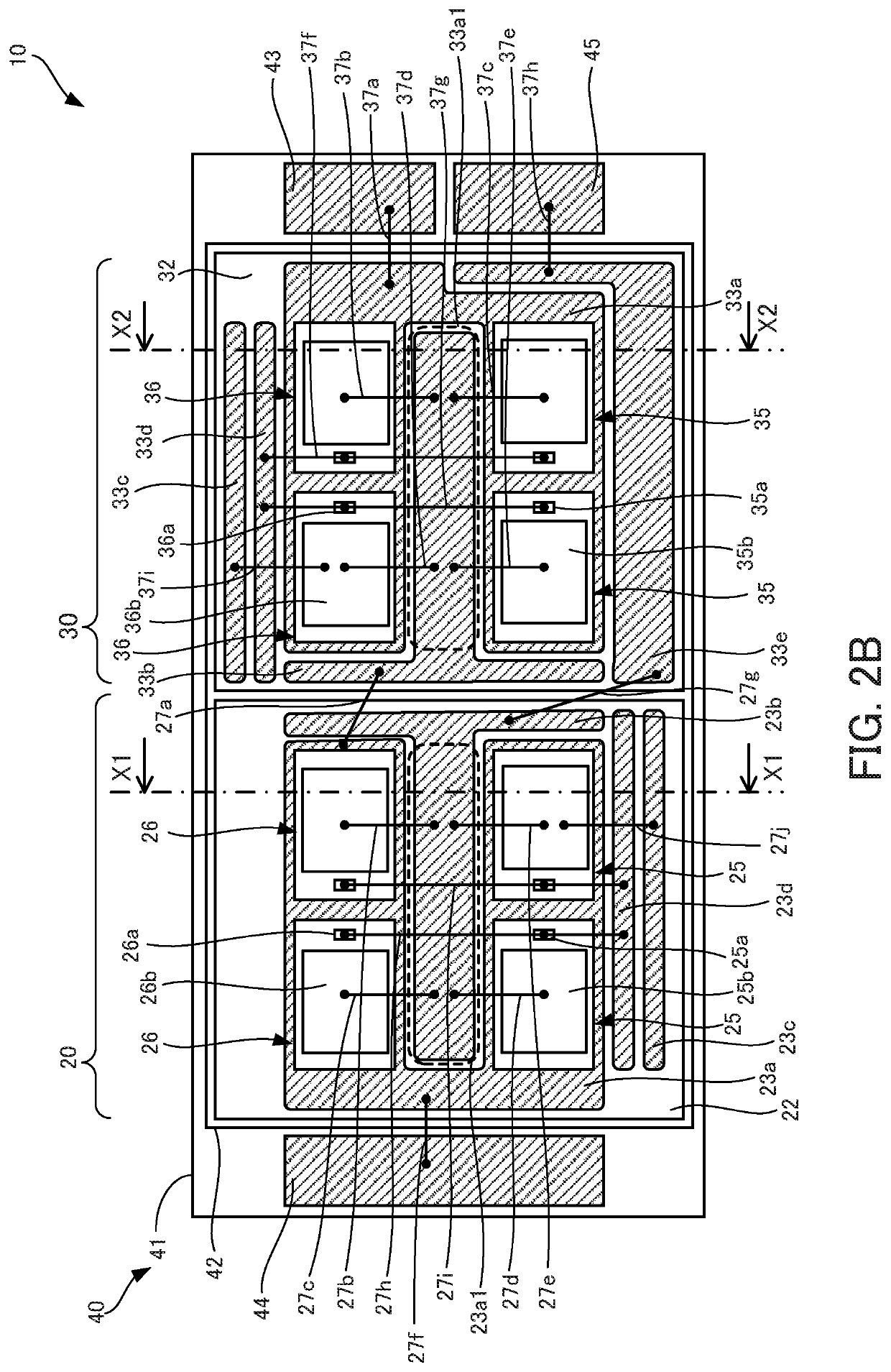
[0020]A semiconductor device of a second embodiment will be described. First a semiconductor device will be described by the use of FIGS. 2A, 2B, 3A and 3B. FIGS. 2A and 2B are plan views of a semiconductor device according to a second embodiment. FIGS. 3A and 3B are sectional views of the semiconductor device according to the second embodiment. FIG. 2A illustrates the case where circuit patterns 23b and 33b are formed in an L shape, and FIG. 2B illustrates the case where the circuit patterns 23b and 33b are formed in a T shape. Except for the circuit patterns 23b and 33b, the semiconductor device 10 illustrated in FIG. 2A has the same configuration as the semiconductor device 10 illustrated in FIG. 2B. FIG. 3A is a sectional view taken along the dot-dash line X1-X1 of FIG. 2A. FIG. 3B is a sectional view taken along the dot-dash line X2-X2 of FIG. 2A.

[0021]A semiconductor device 10 includes a first arm block 20 and a second arm block 30. With the semiconductor device 10 an upper ar...


PUM

PropertyMeasurementUnit
thicknessaaaaaaaaaa
thicknessaaaaaaaaaa
diameteraaaaaaaaaa

Abstract

A semiconductor device having an arm block. The arm block includes a first circuit pattern that, in a plan view of the semiconductor device, has a recess formed thereon that extends inward from a side thereof, the recess forming a disposition area of the semiconductor device, a second circuit pattern having at least a part disposed in the disposition area, and a plurality of semiconductor chips formed on the first circuit pattern. Each semiconductor chip has a positive electrode on a back surface thereof, and a control electrode and a negative electrode on a front surface thereof, the negative electrode being electrically connected to the second circuit pattern by a wiring member.

Description

CROSS-REFERENCE TO RELATED APPLICATION[0001]This application is a continuation application of International Application PCT / JP2019 / 047746 filed on Dec. 6, 2019 which designated the U.S., which claims priority to Japanese Patent Application No. 2019-026543, filed on Feb. 18, 2019, the entire contents of which are incorporated herein by reference.BACKGROUND OF THE INVENTION1. Field of the Invention[0002]The embodiments discussed herein relate to a semiconductor device.2. Background of the Related Art[0003]Semiconductor devices include semiconductor elements such as an insulated gate bipolar transistor (IGBT), a power metal oxide semiconductor field effect transistor (MOSFET), a free wheeling diode (FWD), and a Schottky barrier diode (SBD). Such semiconductor devices include a plurality of semiconductor units including the above semiconductor elements and a radiation plate over which the plurality of semiconductor units are disposed. Such semiconductor devices achieve desired functions...

Claims


Application Information

Patent Timeline
Patent Type & Authority Patents(United States)
IPC IPC(8): H01L23/498H01L23/00H01L25/07H01L25/18
CPCH01L23/49844H01L24/45H01L25/072H01L25/18H01L2924/13055H01L2924/13091H02M7/003H02M7/538H01L24/42H01L2224/49113H01L2224/48137H01L2224/48227H01L2924/19107H01L2224/0603H01L2224/48139H01L24/49H01L24/48H01L24/06H01L2224/04042H01L2224/45124H01L2224/45147H01L2224/45015H01L24/05H01L2224/05554H01L2224/05553H01L2224/49175H01L2924/00014H01L2924/2076
Inventor ICHIKAWA, HIROAKI
Owner FUJI ELECTRIC CO LTD
Why Eureka
Try Eureka