Method and system for analyzing test vectors to determine toggle counts

a test vector and toggle count technology, applied in the field of electric design and testing, can solve the problems of false defects, higher peak test power, ir drops in the power-grid during execution, etc., and achieve the effect of discharging power on the ic, higher average test power, and higher peak test power

Active Publication Date: 2013-12-24
CADENCE DESIGN SYST INC
View PDF8 Cites 8 Cited by
  • Summary
  • Abstract
  • Description
  • Claims
  • Application Information

AI Technical Summary

Benefits of technology

[0004]The toggle activity in the flip-flop is a major component for dissipating power on the IC. Therefore, an increase in the number of toggles during testing will translate into higher average test power during the scan-based test. This is significant, since higher average test power may cause thermal hot-spots, which can result in false defects due to thermal imbalance conditions on the IC chip.
[0005]An increase in localized switching can also result in higher peak test power, which causes IR drops in the power-grid during execution. This can create false defects due to un-factored IR drop conditions on the IC chip and can also cause burn out on the IC chip in extreme cases. Moreover, increased Average and Peak Test Power could result in false defects or yield loss, wherein a good chip is classified as bad chip.
[0006]The present invention is directed to approaches to accurately and efficiently calculate the switching activity (or “toggle count”) when test vectors are applied during manufacturing tests on ATE devices. By accurately calculating the number of flip-flops that toggles during each test clock cycle, one can estimate the power dissipation during testing activity. The toggle count information also helps in predicting power hot-spots on the chip.

Problems solved by technology

This is significant, since higher average test power may cause thermal hot-spots, which can result in false defects due to thermal imbalance conditions on the IC chip.
An increase in localized switching can also result in higher peak test power, which causes IR drops in the power-grid during execution.
This can create false defects due to un-factored IR drop conditions on the IC chip and can also cause burn out on the IC chip in extreme cases.
Moreover, increased Average and Peak Test Power could result in false defects or yield loss, wherein a good chip is classified as bad chip.
The main limitation of scan shift simulation approach is its excessive run time, since the run-time for this approach is almost proportional to the square of the length of the scan chain.
The main limitation with this approach is that it calculates test power by analyzing test vectors using gross estimates, and therefore does not provide accurate toggle counts for each scan cycle.
This approach does not account for scan chain structure in the design, the unbalanced scan chains and the padding bits, and it also does not account for presence of inverters in the scan chains.
In addition, this technique cannot provide the load and unload toggle count at each test clock pulse and does not provide the total number of toggles in each flop.
Moreover, this technique does not account for toggles that occur in overlapped scan due to shifting of unload bit from the unload vector and loading of load bit from the load vector.
Therefore, this technique only provides a first order estimate of power dissipated by a scan vector and does not provide the actual transitions count per test clock cycle.

Method used


Image

  • Method and system for analyzing test vectors to determine toggle counts
  • Method and system for analyzing test vectors to determine toggle counts
  • Method and system for analyzing test vectors to determine toggle counts

Examples


Embodiment Construction

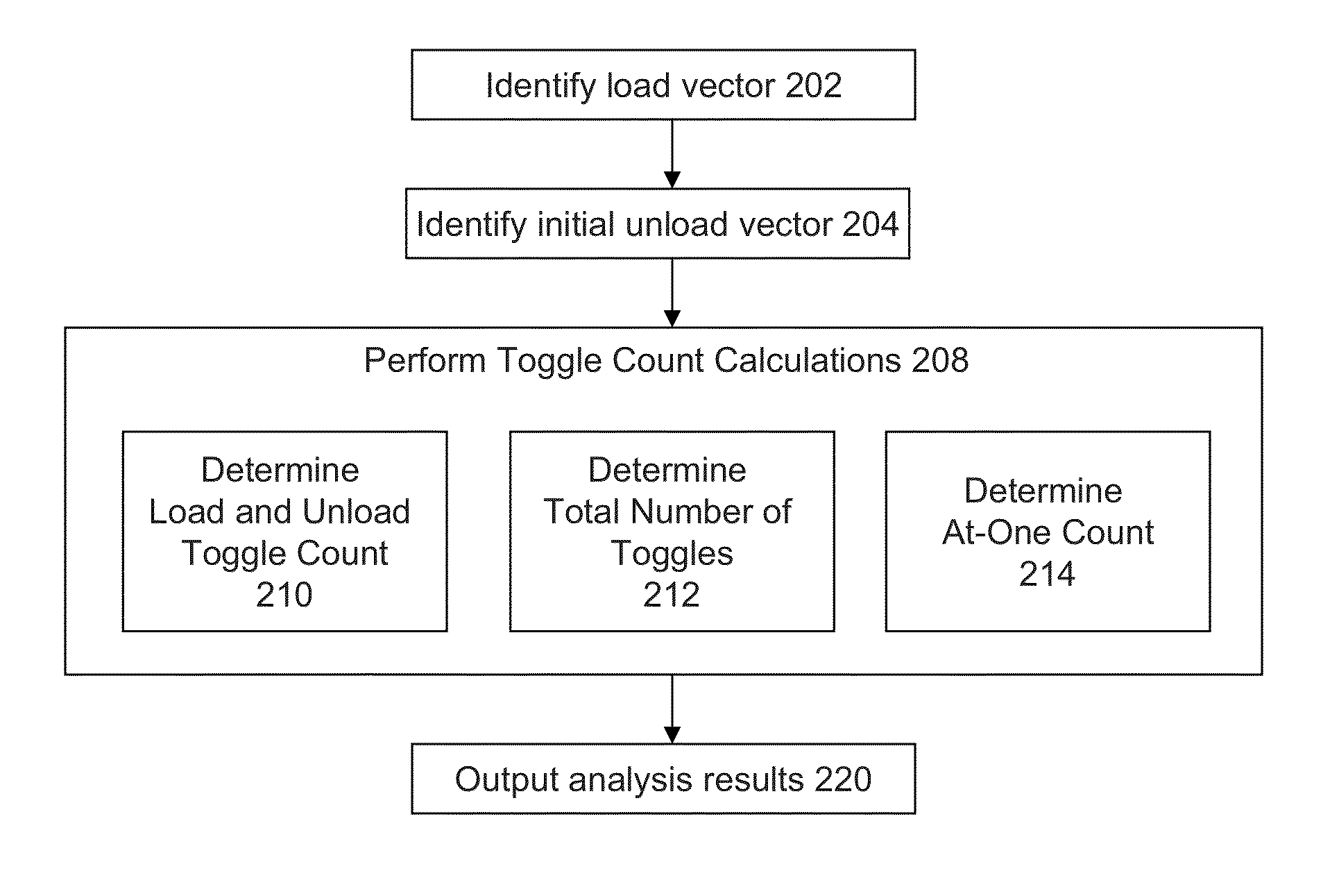
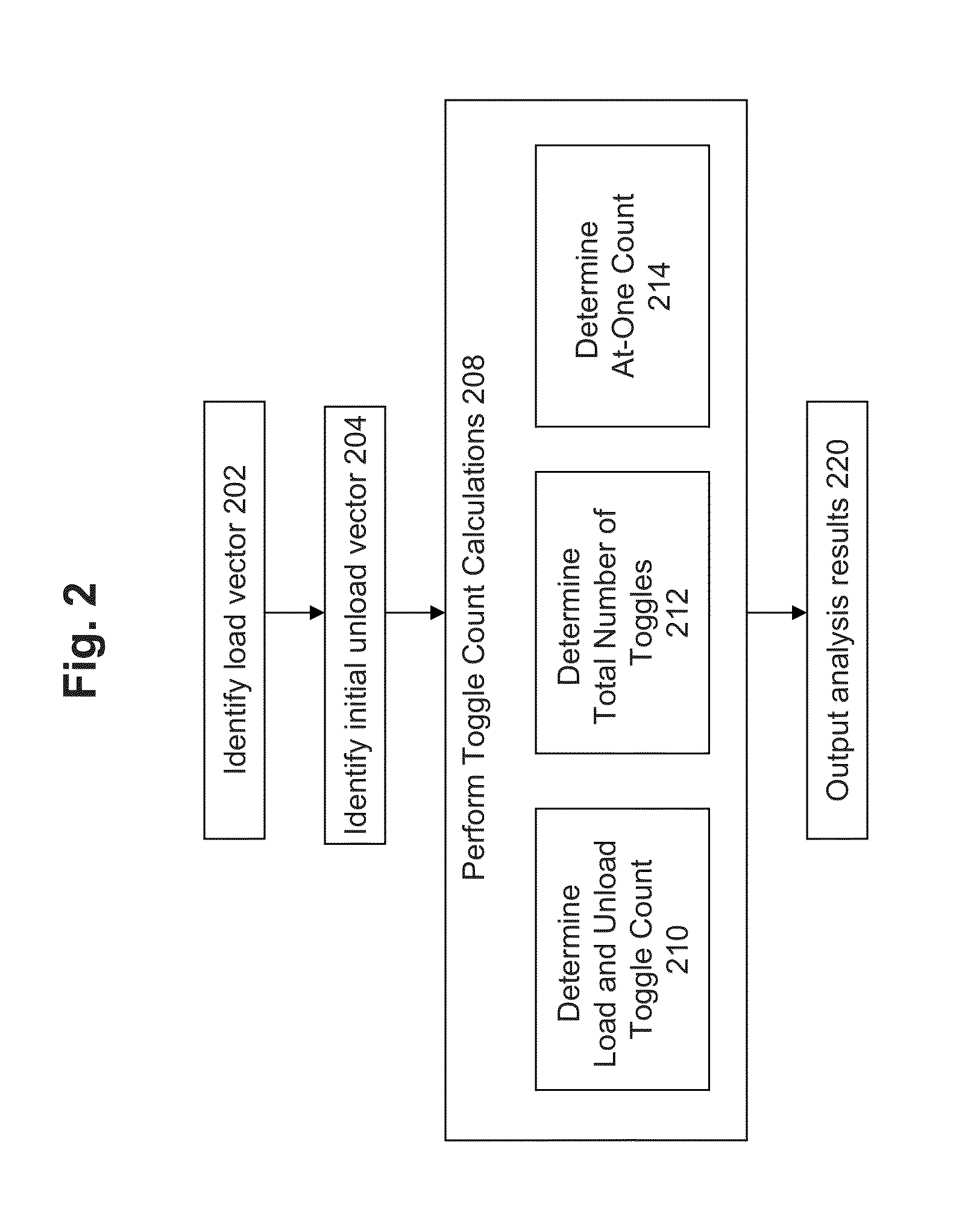
[0025]The present invention is directed to a system, method, and computer program product which provides an efficient and fast approach for analyzing test vectors to perform toggle analysis of tests.

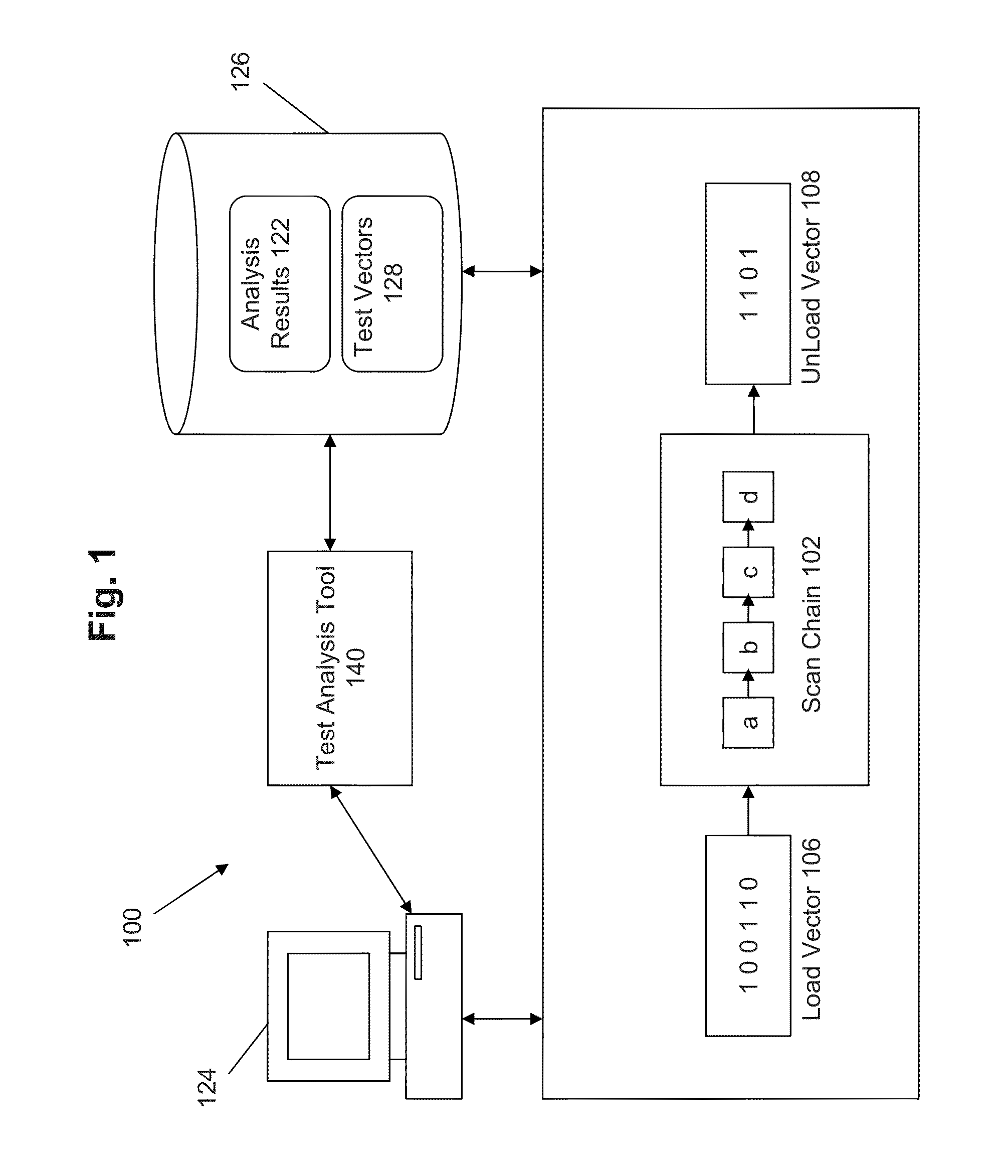
[0026]FIG. 1 illustrates an example system 100 which may be employed in some embodiments of the invention for analyzing test vectors to calculate the switching activity for an electronic design or device. System 100 may include one or more users at one or more user stations 124 that operate the system 100. Such users include, for example, design, test, or verification engineers. User station 124 comprises any type of computing station that may be used to operate, interface with, or implement EDA applications or devices. Examples of such user stations 124 include for example, workstations, personal computers, or remote computing terminals. User station 124 comprises a display device, such as a display monitor, for displaying processing results 122 to users at the user station 124. User st...


PUM


Abstract

A system, method, and computer program product is disclosed that recycle digital assertions for analyzing the test vectors to quickly and accurately calculate the switching activity at each test clock pulse or scan cycle. According to some approaches, load vector data and unload vector data are analyzed to determine toggle counts and switching activity, without requiring simulation to be performed.

Description

FIELD[0001]The invention relates to the field of electrical design and testing.BACKGROUND AND SUMMARY[0002]Automated Testing Equipment (ATE) tools are devices often used to test electronic designs, such as designs of integrated circuit (IC) or application specific integrated circuit (ASIC) products. Scan-based testing is one method of using ATE devices, in which scan logic allows an internal sequential element of the IC, such as a flip-flop, to be to be controlled and observed during testing. Chains of flip-flops (or “flops”) are connected as “scan chains”, and when testing is performed, test vector data that is applied through the scan chain control the sequential state of the flip-flops. After application of the test vector, the response of the scan chains is shifted out of the flip-flops and compared against expected responses to determine whether or not the IC is functioning correctly.[0003]The length of a test vector is equal to the length of longest scan chain, and a test cloc...

Claims


Application Information

Patent Timeline
Patent Type & Authority Patents(United States)
IPC IPC(8): G01R31/28
CPCG01R31/28G01R31/318547G01R31/318575
Inventor KHURANA, RAJESHCHAKRAVADHANULA, KRISHNACHICKERMANE, VIVEK
Owner CADENCE DESIGN SYST INC
Why Eureka
Try Eureka