Method for manufacturing light-emitting device and film formation substrate

a technology of light-emitting devices and film formation substrates, which is applied in thermoelectric devices, instruments, record information storage, etc., can solve the problems of difficult application of the method to a high-definition display device, and the lack of very high-precision film formation, so as to improve the patterning accuracy of an el layer formed over a deposition substra

Inactive Publication Date: 2013-12-31
SHARP KK +1
View PDF81 Cites 5 Cited by
  • Summary
  • Abstract
  • Description
  • Claims
  • Application Information

AI Technical Summary

Benefits of technology

[0012]It is an object of an embodiment of the present invention to provide a method for manufacturing a light-emitting device by which the precision of patterning of an EL layer formed over a deposition substrate can be improved, and a film formation substrate used for the method.
[0023]By application of an embodiment of the present invention, the precision of patterning of an EL layer formed over a deposition substrate can be improved.

Problems solved by technology

However, this method does not provide very high-precision film formation and thus requires that the distance between pixels be designed to be large and that the width of a partition (a bank) formed of an insulator between pixels be large.
Therefore, application of the method to a high-definition display device is difficult.

Method used


Image

  • Method for manufacturing light-emitting device and film formation substrate
  • Method for manufacturing light-emitting device and film formation substrate
  • Method for manufacturing light-emitting device and film formation substrate

Examples


embodiment 1

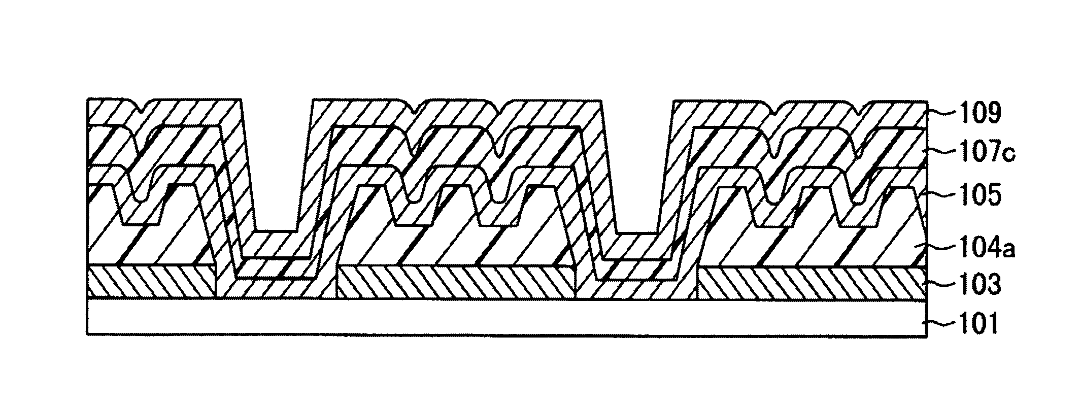
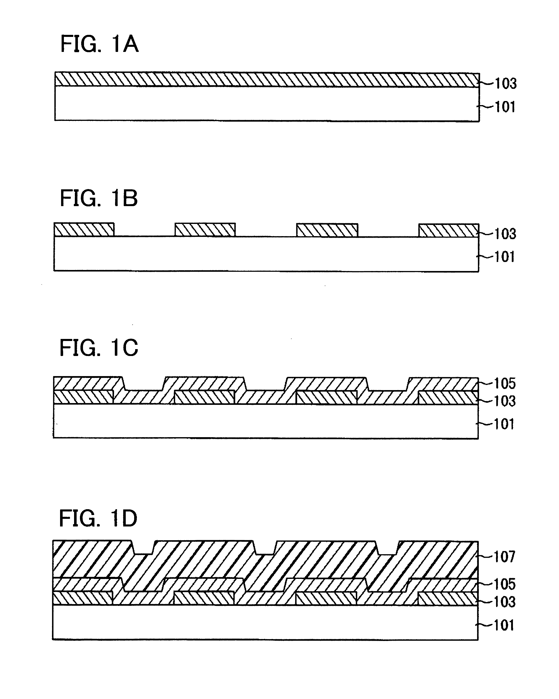
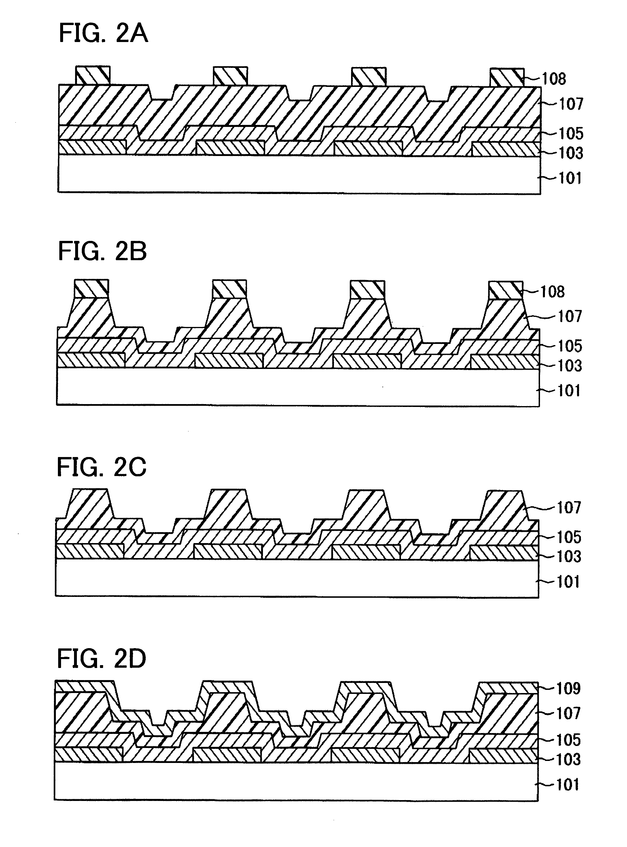
[0033]FIGS. 1A to 1D and FIGS. 2A to 2D are cross-sectional views illustrating a method for manufacturing a film formation substrate according to an embodiment of the present invention. FIGS. 3A and 3B are cross-sectional views illustrating a method for manufacturing a light-emitting device using a film formation substrate illustrated in FIG. 2D.

[0034]A reflection layer 103 is formed over a first substrate 101 as illustrated in FIG. 1A, and then an opening is formed in the reflective layer 103 as illustrated in FIG. 1B.

[0035]The first substrate 101 is the supporting substrate for the reflective layer, the light absorption layer, the heat insulating layer, and the like, and transmits irradiation light used for depositing the material layer onto a deposition substrate in a manufacturing process of a light-emitting device. Therefore, the first substrate 101 preferably has high light transmittance. Specifically, when lamp light or laser light is used in order to deposit the material lay...

embodiment 2

[0092]FIGS. 6A to 6D are cross-sectional views illustrating a method for manufacturing a film formation substrate according to an embodiment of the present invention. FIGS. 7A and 7B are cross-sectional views illustrating a method for manufacturing a light-emitting device using the film formation substrate illustrated in FIG. 6D. Note that in FIGS. 6A to 6D and FIGS. 7A and 7B, the same portions as those in FIGS. 1A to 1D, FIGS. 2A to 2D, FIGS. 3A and 3B, FIGS. 4A to 4C, and FIG. 5 are denoted by the same reference numerals and the description thereof is omitted.

[0093]As illustrated in FIG. 6A, a reflective layer 103 is formed over a first substrate 101 and a heat insulating layer 104 is formed over the reflective layer 103.

[0094]Next, as illustrated in FIG. 6B, a resist film is formed over the heat insulating layer 104 and this resist film is exposed to light and developed, so that a resist pattern 106 is formed over the heat insulating layer 104.

[0095]After that, as illustrated in...


PUM

PropertyMeasurementUnit
sizeaaaaaaaaaa
sizeaaaaaaaaaa
reflectanceaaaaaaaaaa

Abstract

In a method for manufacturing a light-emitting device according to an embodiment of the present invention, one surface of a first substrate including a reflective layer including an opening, a light absorption layer formed over the reflective layer to cover the opening in the reflective layer, a protective layer formed over the light absorption layer and including a groove at a position overlapped with the opening in the reflective layer, and a material layer formed over the protective layer and a deposition surface of a second substrate are disposed to face each other and light irradiation is performed from the other surface side of the first substrate, so that an EL layer is formed in a region on the deposition surface of the second substrate, which is overlapped with the opening in the reflective layer.

Description

TECHNICAL FIELD[0001]The present invention relates to a light-emitting device and a method for manufacturing the light-emitting device. The present invention also relates to a film formation substrate used for film formation of a material which can be deposited onto a substrate.BACKGROUND ART[0002]An organic compound can take a wider variety of structures compared with an inorganic compound, and it is possible to synthesize a material having a variety of functions by appropriate molecular-design of an organic compound. Owing to these advantages, photo electronics and electronics which use a functional organic material have been attracting attention in recent years.[0003]Examples of electronic devices in which organic compounds are used as functional organic materials include solar cells, light-emitting elements, organic transistors, and the like. These are devices taking advantage of electric properties and optical properties of the organic compound. Among them, in particular, a lig...

Claims


Application Information

Patent Timeline
Patent Type & Authority Patents(United States)
IPC IPC(8): H01L33/00
CPCH01L51/0013H01L51/56C23C14/048H10K71/18H10K71/40H10K71/00
Inventor AOYAMA, TOMOYAYOKOYAMA, KOHEITSURUOKA, RENAUCHIDA, HIDEKISONODA, TORUINOUE, SATOSHI
Owner SHARP KK
Why Eureka
Try Eureka