Light emitting apparatus, method of driving light emitting apparatus, and electronic apparatus

a technology of light emitting apparatus and light emitting transistor, which is applied in the direction of electric digital data processing, instruments, computing, etc., can solve the problems of complex configuration, difference in target value or non-uniformity among pixels, and errors in driving transistor characteristics, etc., to achieve sufficient time period and simplify the effect of configuration

Active Publication Date: 2014-01-07
SEIKO EPSON CORP
View PDF5 Cites 9 Cited by
  • Summary
  • Abstract
  • Description
  • Claims
  • Application Information

AI Technical Summary

Benefits of technology

[0008]An advantage of some aspects of the invention is to simplify a configuration for performing the initialization or compensation operation and to secure a sufficient time period for writing a data voltage.
[0013]In other words, according to the invention, there is an advantage in that it is possible to simplify the configuration for performing the initialization or compensation operation and to secure a sufficient time period for writing the data voltage.
[0014]In the light emitting apparatus according to the above aspect of the invention, the first, second, and third voltages may be set so that the light emitting device does not emit light in the initialization period, the compensation period, and the selection period. If the light emitting device emits light in a time period (for example, a time period corresponding to the initialization period or the compensation period) before the start of the light emitting period, there is a problem in that a contrast of a displayed image deteriorates. According to the aspect, the light emitting device can be securely maintained in the off state (light non-emitting state) in a time period before the start of the light emitting period. Therefore, there is an advantage in that it is possible to suppress the deterioration in the contrast of the displayed image.
[0018]In the above aspect, a demultiplexer method in which the data voltages time-divisionally supplied to each of the image signal lines are distributed to the data lines included in the block corresponding to the image signal line by the selection unit corresponding to the image signal line is employed. Therefore, the total number of the image signal lines that are the output wire lines of the driving circuit may be smaller than the total number of the data lines. In other words, there is an advantage in that the number of the output wire lines of the driving circuit can be reduced.

Problems solved by technology

In a light emitting apparatus in which a driving transistor controls a driving current supplied to a light emitting device, there is a problem of errors in a characteristic of the driving transistor (difference from a target value or non-uniformity among pixels).
However, in the technology disclosed in JPA-2008-9198, since a large number of signal lines and transistors are provided to perform an initialization or compensation operation, there is a problem in that the configuration is complicated.
However, in the technology disclosed in JPA-2007-310311, in the time period (one horizontal scan time period) in which the selection transistor 3A is set to the ON state, since the reference voltage V0 and the data voltage Vin are configured to be time-divisionally supplied to the data line DTL101, there is s a problem in that it is difficult to secure a sufficient time period for writing the data voltage in the one horizontal scan time period.
If the light emitting device emits light in a time period (for example, a time period corresponding to the initialization period or the compensation period) before the start of the light emitting period, there is a problem in that a contrast of a displayed image deteriorates.

Method used


Image

  • Light emitting apparatus, method of driving light emitting apparatus, and electronic apparatus
  • Light emitting apparatus, method of driving light emitting apparatus, and electronic apparatus
  • Light emitting apparatus, method of driving light emitting apparatus, and electronic apparatus

Examples


first embodiment

A: First Embodiment

A-1: Configuration and Operations of Light Emitting Apparatus

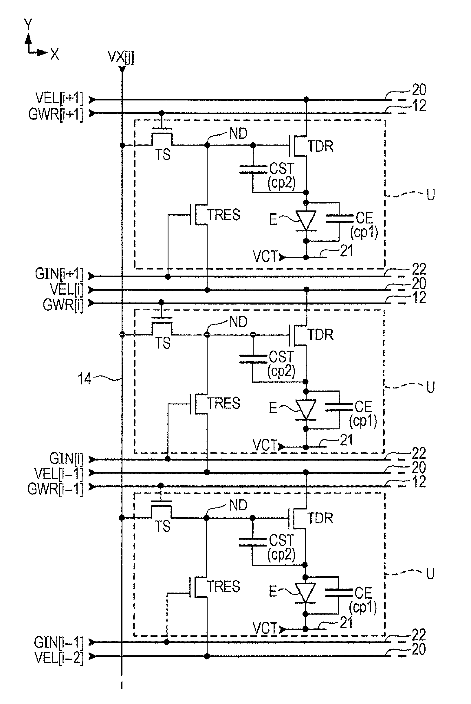
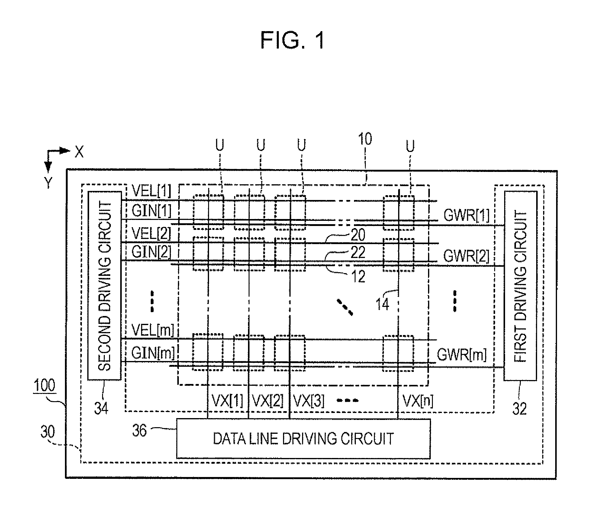
[0045]FIG. 1 is a block diagram illustrating a light emitting apparatus 100 according to a first embodiment of the invention. The light emitting apparatus 100 is a display apparatus of displaying an image, which is mounted on an electronic apparatus. As shown in FIG. 1, the light emitting apparatus 100 includes a device unit 10 where a plurality of pixel circuits U are disposed and a driving circuit 30 which drives the pixel circuits U. The driving circuit 30 includes a first driving circuit 32, a second driving circuit 34, and a data line driving circuit 36. The driving circuit 30 is distributively mounted on, for example, a plurality of integrated circuits. At least a portion of the driving circuit 30 may be configured with thin film transistors which are formed together with the pixel circuits U on a substrate.

[0046]In the device unit 10, m scan lines 12 extending in the X direction, m first feed line...

second embodiment

B: Second Embodiment

B-1: Principle of Driving

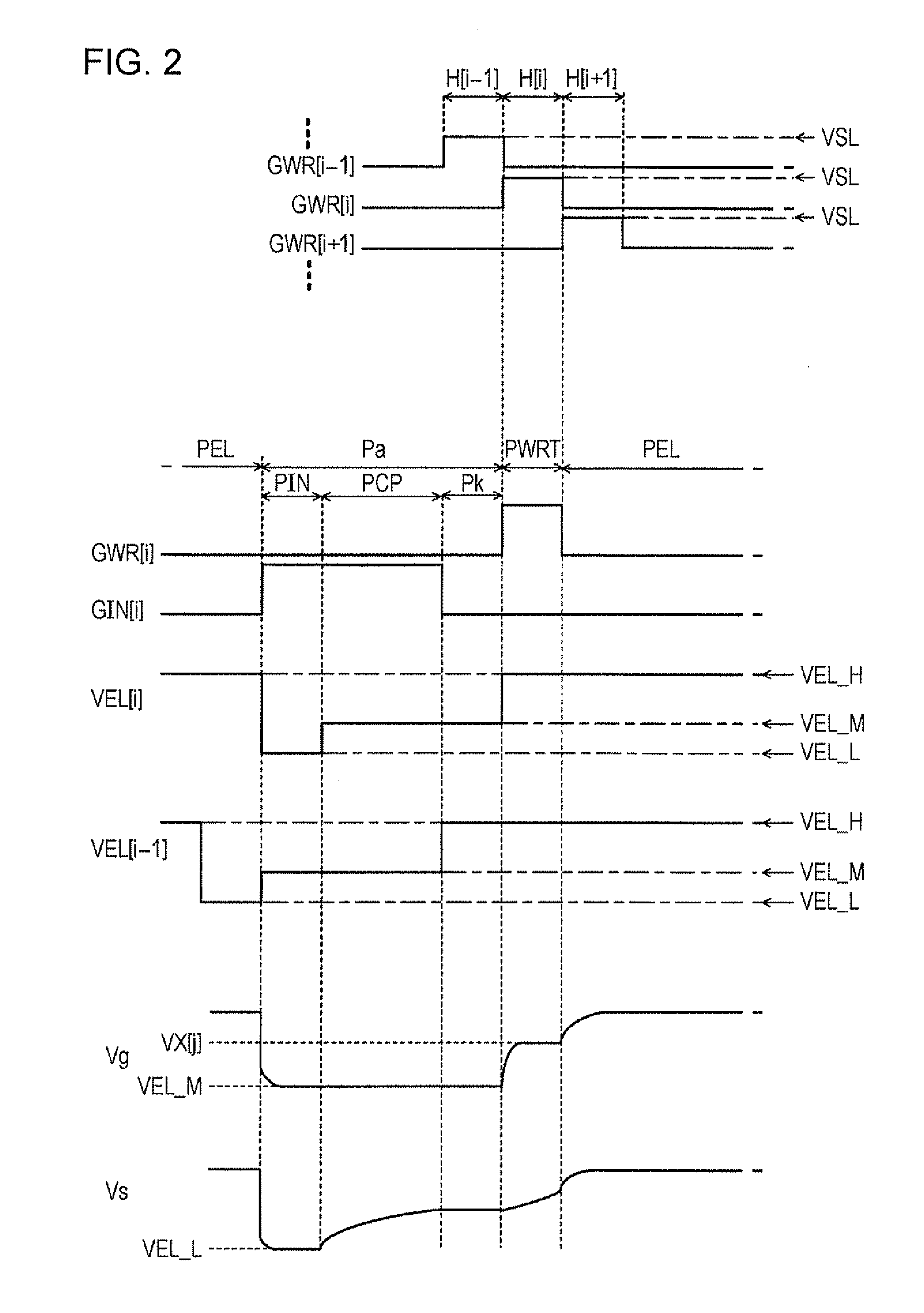
[0079]A second embodiment is different from the aforementioned first embodiment in that the data voltages VX[1] to VX[n] output from the data line driving circuit 36 to the data lines 14 are varied with the one horizontal scan time period H as a period as time elapses. Now, a principle used for driving pixel circuits according to the second embodiment is described before the detailed description of the embodiment. As shown in FIG. 12, a circuit where an N channel type driving transistor TDR and a capacitance CE (capacitance value cp1) are disposed in series in a path connecting a first feed line 20 and a second feed line 21 is considered.

[0080]The voltage VEL is supplied to the first feed line 20, and the voltage VCT (VCT21. The drain of the driving transistor TDR is connected to the first feed line 20, and the capacitance CE is interposed between the source of the driving transistor TDR and the second feed line 21. A capacitance device C...

third embodiment

C: Third Embodiment

[0097]FIG. 15 is a block diagram illustrating a light emitting apparatus 100 according to a third embodiment. In the third embodiment, 3n data lines 14 are grouped into n blocks B (B[1] to B[n]) in units of three adjacent lines. Herein, m red pixel circuits U arrayed in the Y direction are connected to the first data line 14 of each of the blocks B[1] to B[n]. Similarly, m green pixel circuits U are connected to the second data line 14 of each of the blocks B[1] to B[n], and m blue pixel circuits U are connected to the third data line 14. In other words, the m pixel circuits U arrayed in the Y direction correspond to the same color (in a stripe array). In addition, the configuration of the array of each of the display colors can be arbitrarily changed.

[0098]In addition, as shown in FIG. 15, the light emitting apparatus 100 according to the embodiment further includes n image signal lines 16, which are disposed in one-to-one correspondence with the n blocks B[1] to...


PUM


Abstract

Provided is a light emitting apparatus where each pixel circuit is provided with the reset transistor, which is disposed between the node of the pixel circuit and the first feed line corresponding to the adjacent pixel circuit in the second direction as viewed from the pixel circuit. In addition, in the initialization period before the selection period, in which the scan line corresponding to the pixel circuit is selected, and in the compensation period, the reset transistor of the pixel circuit is set to the ON state, and the values of the power supply voltages output to the first feed line corresponding to the pixel circuit and the first feed line corresponding to the adjacent pixel circuit in the second direction as viewed from the pixel circuit are variably controlled, so that the initialization or compensation operation of the pixel circuit is performed.

Description

BACKGROUND[0001]1. Technical Field[0002]The present invention relates to a light emitting apparatus, a method of driving a light emitting apparatus, and an electronic apparatus.[0003]2. Related Art[0004]In a light emitting apparatus in which a driving transistor controls a driving current supplied to a light emitting device, there is a problem of errors in a characteristic of the driving transistor (difference from a target value or non-uniformity among pixels). JPA-2008-9198 and JP-A-2007-310311 discloses a technology for compensating for an error of a threshold voltage or a mobility of the driving transistor by setting a gate-source voltage of the driving transistor to a threshold voltage of the driving transistor and then changing to a voltage according to gradation.[0005]FIG. 21 is a circuit diagram illustrating a configuration of a pixel circuit P0 disclosed in JP-A-2008-9198. In the initialization period, the transistors Tr2 and Tr3 are set to the ON state, so that the gate-so...

Claims


Application Information

Patent Timeline
Patent Type & Authority Patents(United States)
IPC IPC(8): G06F3/038
CPCG09G3/3233G09G2310/0251G09G3/3266G09G2310/0297
Inventor ISHIGURO, HIDETOYATABE, SATOSHI
Owner SEIKO EPSON CORP
Why Eureka
Try Eureka