

Common mode filter
a filter and common mode technology, applied in the direction of coils, transformers/inductance details, inductances, etc., can solve the problems of large volume of electronic components and affect process variables, and achieve the effect of simple structural configuration
- Summary
- Abstract
- Description
- Claims
- Application Information
AI Technical Summary
Benefits of technology
Problems solved by technology
Method used
Image

Examples
first embodiment
The First Embodiment
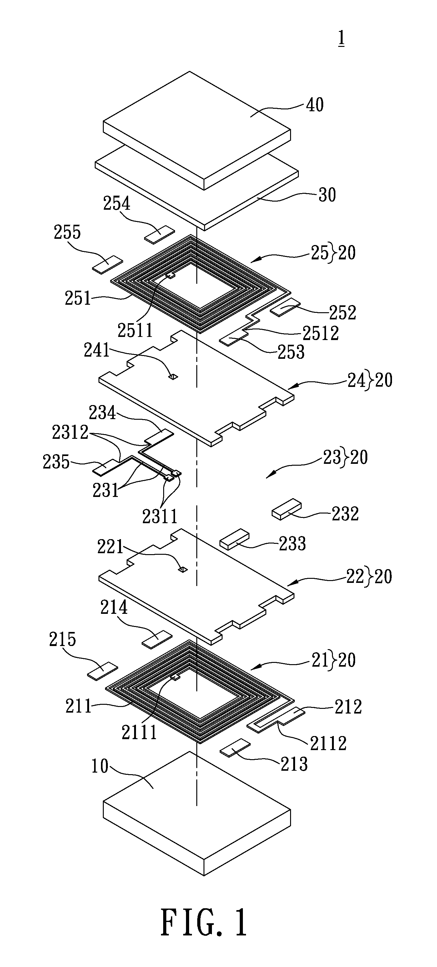
[0026]Please refer to FIG. 1, The thin-film common mode filter 1 includes a non-magnetic insulating substrate 10, a stacked-layer structure 20, an insulating layer 30, and a magnetic layer 40.
[0027]The stacked-layer structure 20 is arranged on the non-magnetic insulating substrate 10 and includes a first coil body 21, a first electric insulating layer 22, a coil leading layer 23, a second electric insulating layer 24, and a second coil body 25 in sequential order. The magnetic layer 40 covering the stacked-layer structure 20 by the insulating layer 30 interposed therebetween to increase inductance effect of the common mode filter 1. In this embodiment, the insulating layer 30 can be, but not limited to, an adhesive layer.
[0028]The specific features of the stacked-layer structure 20 are described as follows. The first coil body 21 includes a first spiral coil 211, a first electrode 212, a second electrode 213, a third electrode 214, and a fourth electrode 215. Mor...
second embodiment
The Second Embodiment
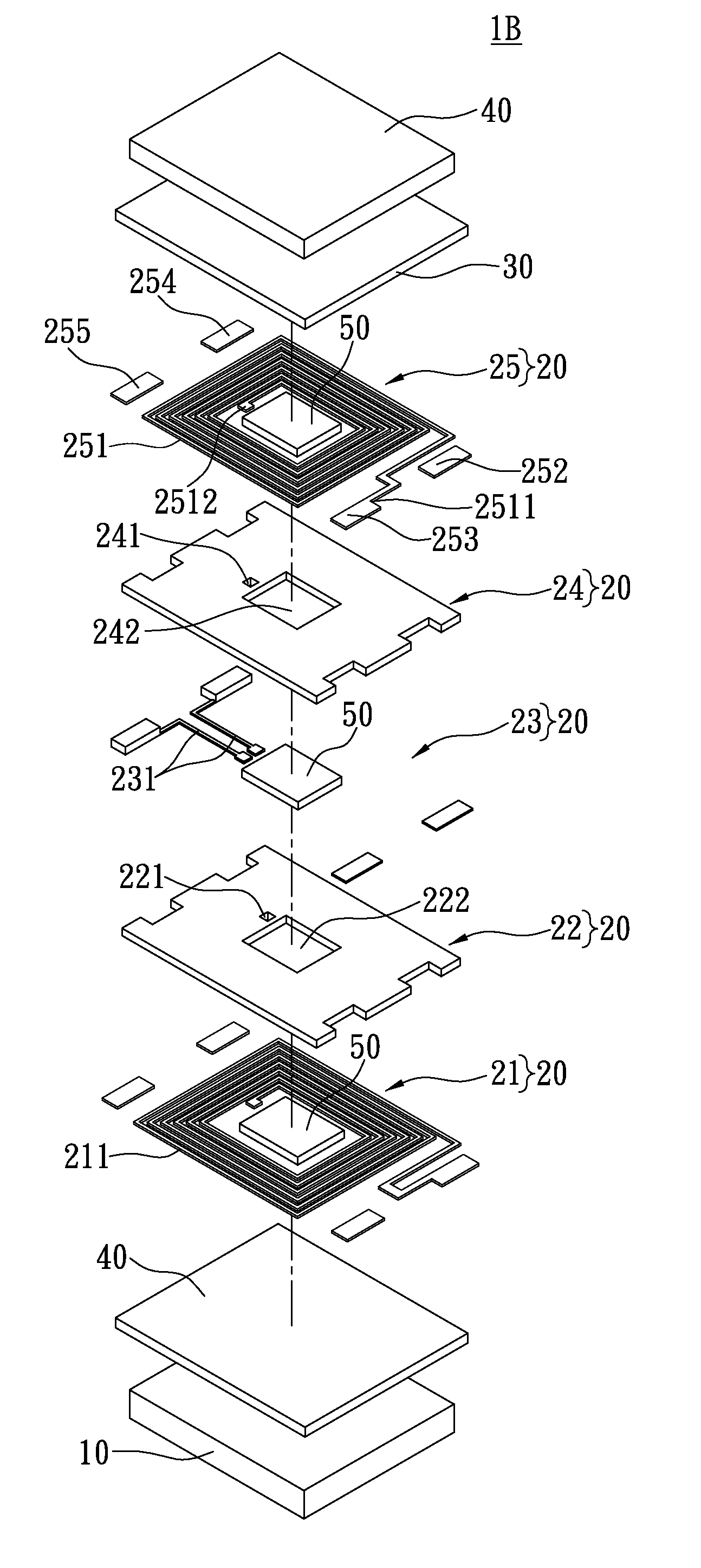
[0038]Please refer to FIG. 3A, which shows a common mode filter in accordance to the second embodiment of the instant disclosure. The difference in the second embodiment is that the common mode filter 1A further comprises another magnetic layer 40. Said another magnetic layer 40 is arranged between the non-magnetic insulating substrate 10 and the stacked-layer structure 20.
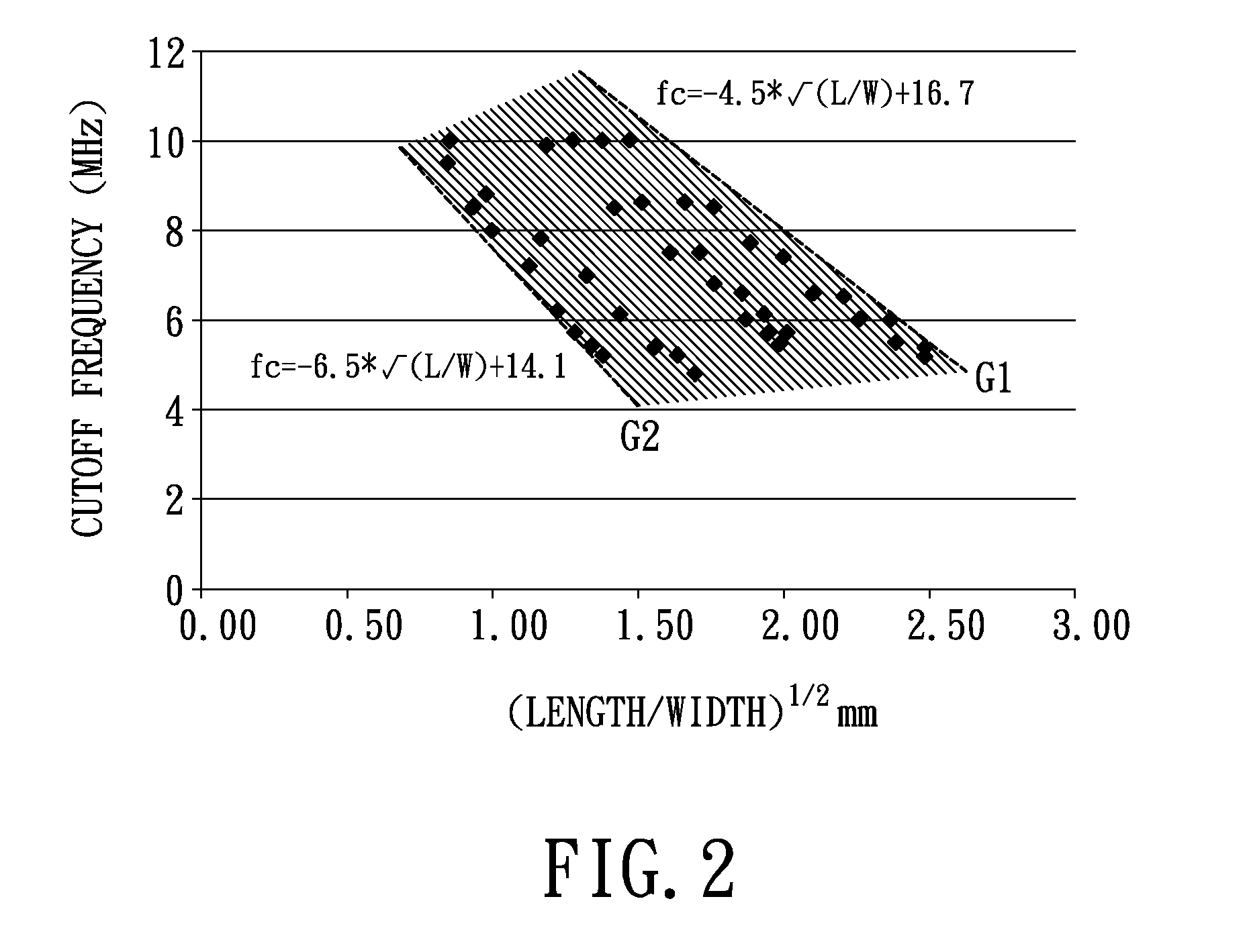
[0039]Concretely speaking, said another magnetic layer 40 is arranged between the non-magnetic insulating substrate 10 and the first coil body 21 to achieve better eliminating efficiency of the common mode noise. Similarly, a width W (mm) and a length L (mm) of at least one spiral coil in the first and second spiral coils 211, 251 satisfy the relational expression of:
[(14.1−fc) / 6.5]2<L / W−fc) / 4.5]2
where fc (MHz) is the cutoff frequency of a differential-mode signal. Thereby, the cutoff frequency generated by the thin-film common mode filter 1A is about 4 to 10 MHz such that the thin-film co...
third embodiment
The Third Embodiment
[0040]Please refer to FIG. 3B, which shows a common mode filter in accordance to the third embodiment of the instant disclosure. The difference in the third embodiment is that the common mode filter 1B comprises a plurality of magnetic members 50 having the advantages of high resistance and low eddy current loss in a wild range of frequencies. In this embodiment, the magnetic members 50 can be, but not limited to ferrite cores.
[0041]In addition, each of the first and second electric insulating layers 22, 24 has a through-hole 222, 242 formed thereon near the first and the second conducting structures 221, 241 respectively. The magnetic members 50 respectively arranged inside the first, second spiral coils 211, 251 and near one end of the L-shaped coils 231 through the through-holes 222, 242 to increase the magnetic field intensity between the first and the second coil body 21, 25 (means that cross magnetic field intensity between the first and the second spiral c...
PUM
| Property | Measurement | Unit |
|---|---|---|
| cutoff frequency | aaaaa | aaaaa |
| cutoff frequency | aaaaa | aaaaa |
| magnetic | aaaaa | aaaaa |
Abstract
Description
Claims
Application Information