Manufacturing method of semiconductor device

a manufacturing method and semiconductor technology, applied in the direction of instruments, basic electric elements, digital data processing details, etc., can solve the problems of inability to use identification codes in follow-up surveys, difficult for conventional product management methods to quickly investigate, etc., and achieve the effect of quick anti-defect measures

Active Publication Date: 2014-02-11
RENESAS ELECTRONICS CORP
View PDF8 Cites 3 Cited by
  • Summary
  • Abstract
  • Description
  • Claims
  • Application Information

AI Technical Summary

Benefits of technology

[0011]It is an object of the present invention to provide a management method capable of quickly investigating the cause of a defect of a semiconductor product.
[0016]According to the preferred aspect of the present invention, conditions for manufacturing a semiconductor package stored in a computer can be traced in an instant by reading a bar code affixed to the surface of the semiconductor package, so that it is possible to take an anti-defect measure quickly.

Problems solved by technology

In recent years, however, the types of semiconductor products are diversified and semiconductor product manufacturing steps are also diversified and complicated, so in the event of occurrence of a defect of a semiconductor product, it is difficult for the conventional product management methods to quickly investigate the cause of the defect.
This identification code cannot be utilized in the follow-up survey for investigating the cause of a defect developed in the post-process because it does not contain any information on manufacturing conditions in the post-process (assembling process).

Method used


Image

  • Manufacturing method of semiconductor device
  • Manufacturing method of semiconductor device
  • Manufacturing method of semiconductor device

Examples


first embodiment

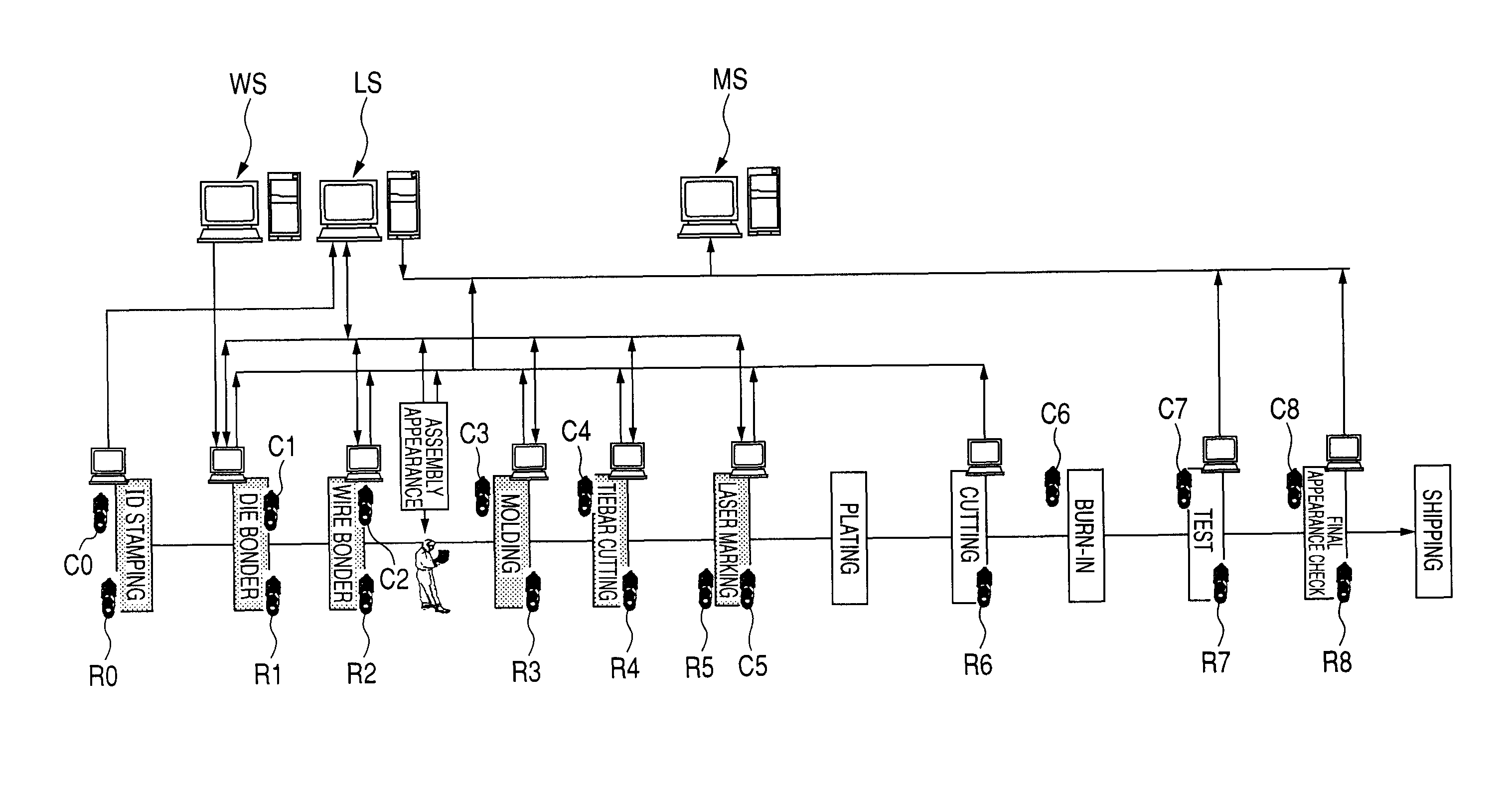
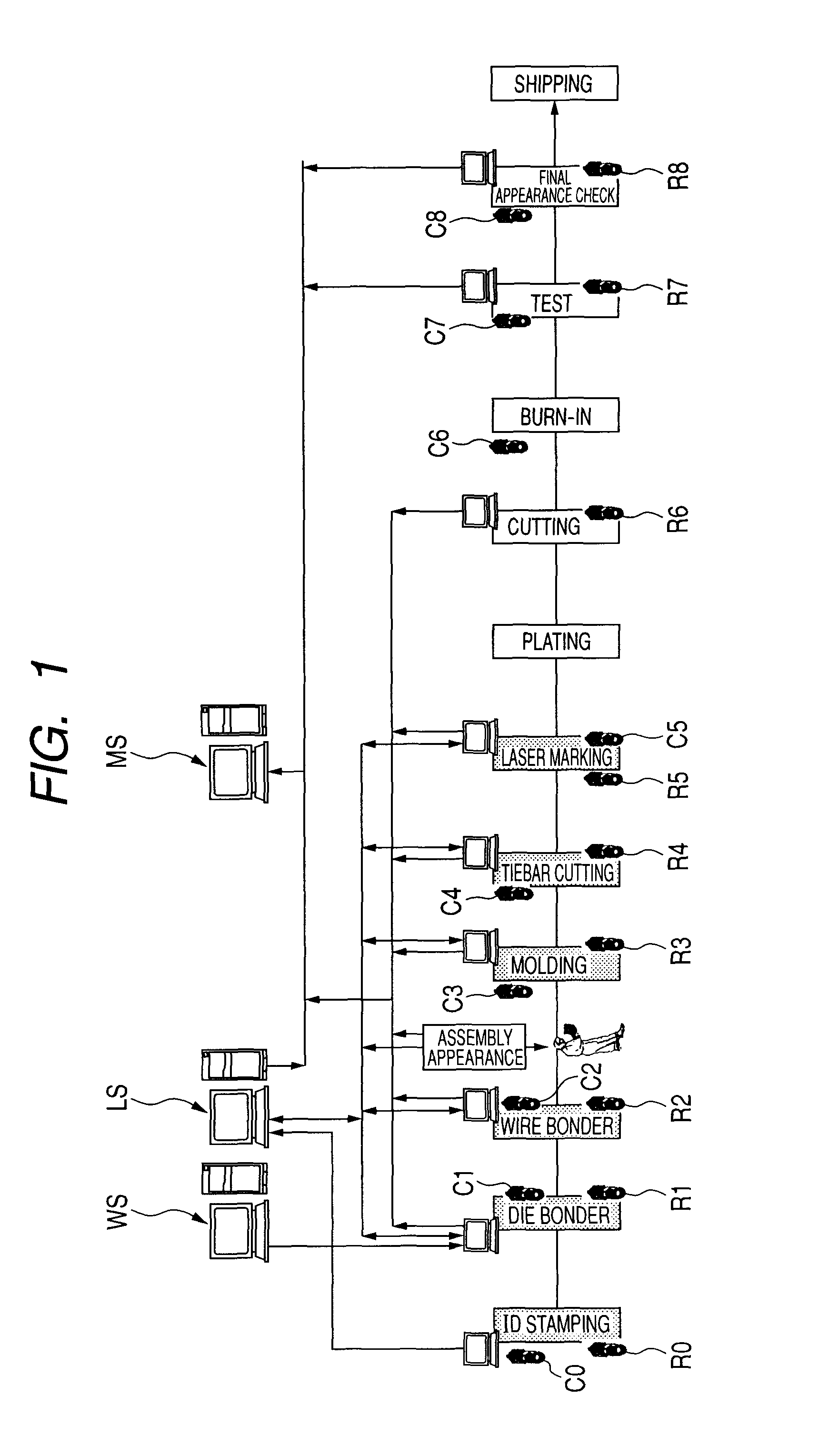
[0046]In this embodiment the present invention is applied to the manufacture of a QFP (Quad Flat Package) which is a kind of a semiconductor package. FIG. 1 is an entire flow chart showing a manufacturing process for the QFP.

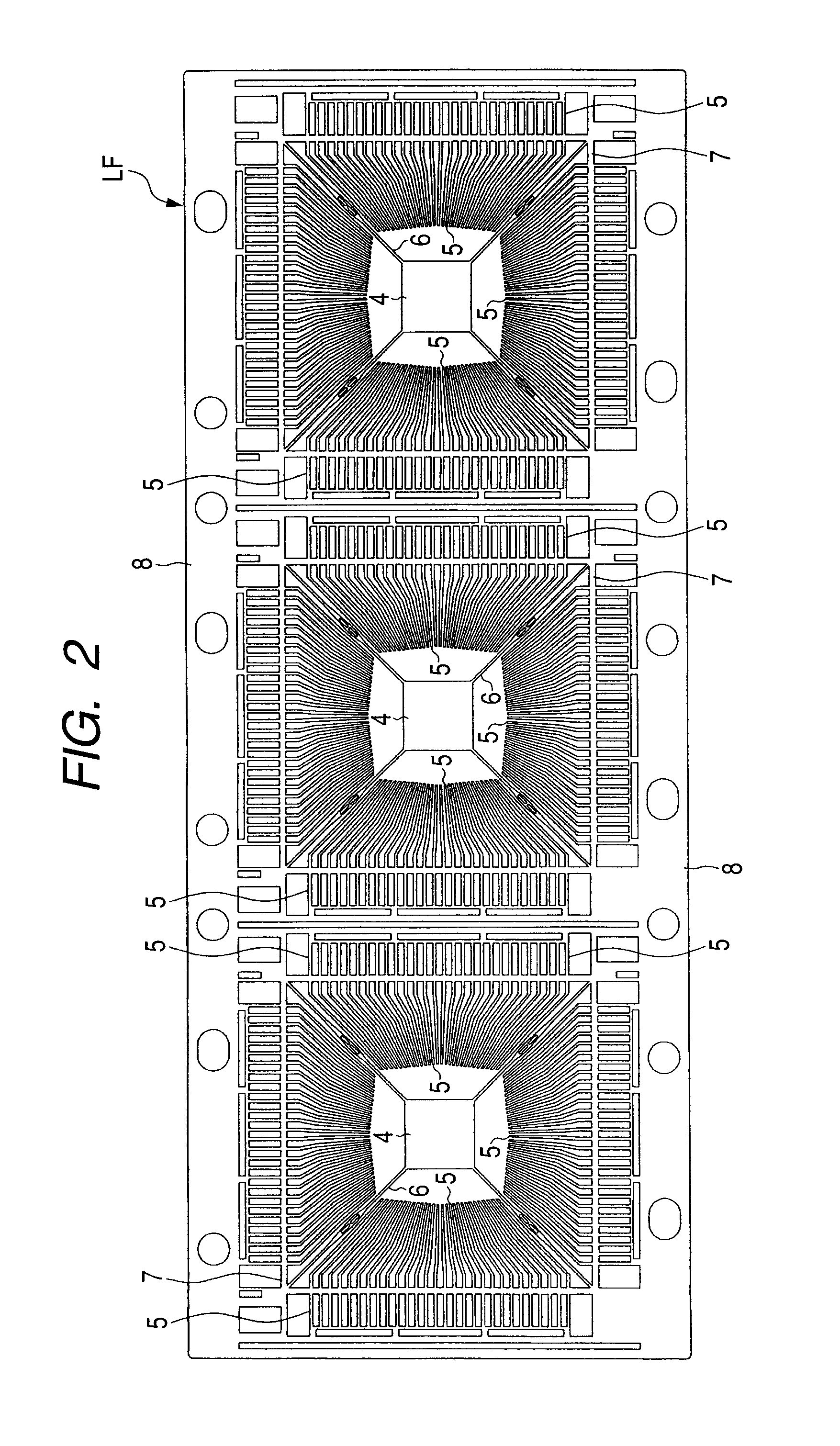
[0047]For manufacturing the QFP, first a lead frame shown in FIG. 2 and a semiconductor wafer shown in FIG. 3 are provided as base members (chip mounting members).

[0048]The lead frame LF shown in FIG. 2 is formed of copper (Cu) or copper alloy and comprises a plurality of device areas (areas which will become semiconductor devices) and an outer frame portion 8 positioned outside the device areas. Each device area includes a chip mounting area (die pad, chip mounting portion) 4 as a portion for mounting a semiconductor chip, a plurality of leads 5 formed around the chip mounting area 4, a plurality of suspending leads 6 formed integrally with the chip mounting area 4, and tiebars 7 formed integrally with both leads 5 and suspending leads 6. The leads 5, suspendin...

second embodiment

[0104]In this embodiment the present invention is applied to the manufacture of a CSP (Chip Size Package) which is a kind of a semiconductor package. FIG. 18 is an entire flow chart showing a manufacturing process for the CSP. As to the same contents, such as configuration, conditions and effects, as in the first embodiment, explanations thereof will be omitted.

[0105]For manufacturing the CSP, first as base members (chip mounting members), there are provided a wiring substrate (map substrate) 20 formed with a plurality of device areas such as that shown in FIGS. 19 and 20, as well as a semiconductor wafer. FIG. 19 is an entire plan view showing a surface (upper surface, main surface) of the map substrate 20 and FIG. 20 is an entire plan view showing a back surface (lower surface, packaging surface) of the map substrate 20.

[0106]The map substrate 20 is a large-sized wiring substrate which serves as a matrix of a wiring substrate 25 of the CSP to be described later. A plurality of wir...


PUM


Abstract

A management method is able to quickly investigate the cause of a defect generated in a semiconductor product manufacturing process. Manufacturing conditions in various QFP manufacturing steps are stored in a main server while correlating them with an identification number of the QFP, and a two-dimensional bar code corresponding to the identification number is stamped to the surface of the QFP. In the event of occurrence of a defect of the QFP, the manufacturing conditions for the QFP stored in the main server can be traced in an instant by reading the two-dimensional bar code of the QFP and thereby specifying the identification number.

Description

CROSS-REFERENCE TO RELATED APPLICATIONS[0001]The disclosure of Japanese Patent Application No. 2009-217825 filed on Sep. 18, 2009 including the specification, drawings and abstract is incorporated herein by reference in its entirety.BACKGROUND OF THE INVENTION[0002]The present invention relates to a manufacturing method of a semiconductor device. Particularly, the present invention is concerned with a semiconductor manufacturing technique capable of quickly investigating the cause of a defect generated in a semiconductor device manufacturing process.[0003]The semiconductor device manufacturing process broadly comprises a pre-process (wafer process) in which integrated circuits are formed on a main surface (integrated circuit-forming surface) of a semiconductor wafer, e.g., a single crystal silicon wafer, by combining photolithography technique, CVD technique, sputtering technique and etching technique and a post-process (assembling process) in which the semiconductor wafer formed wi...

Claims


Application Information

Patent Timeline
Patent Type & Authority Patents(United States)
IPC IPC(8): G06F19/00
CPCH01L2924/01074H01L24/48H01L23/544H01L2224/97H01L2924/01027H01L2924/15311H01L2924/014H01L24/97H01L2924/01029H01L2223/54413H01L2224/32245H01L2224/45144H01L2224/32014H01L2223/54486H01L2924/01005H01L2924/01033H01L2924/01082H01L2924/01079H01L2224/48091H01L2924/10253H01L2224/73265H01L2223/54433H01L2224/92247H01L2924/01006H01L2924/01078H01L2224/49171H01L21/67294H01L2924/14H01L2224/48247H01L21/561H01L2224/45015H01L2924/181H01L2924/00014H01L2924/12042H01L24/45H01L2224/05554H01L24/49H01L2224/85H01L2924/00H01L2224/05599H01L2924/00012
Inventor YOKOSAWA, KAORU
Owner RENESAS ELECTRONICS CORP
Why Eureka
Try Eureka