Acoustic wave device

a technology of acoustic waves and silicon oxide films, applied in piezoelectric/electrostrictive/magnetostrictive devices, piezoelectric/electrostriction/magnetostriction machines, electrical equipment, etc., can solve the problem that the use of silicon oxide films doped with b fails to improve a temperature dependence of frequency sufficiently

Active Publication Date: 2014-03-04
TAIYO YUDEN KK
View PDF6 Cites 7 Cited by
  • Summary
  • Abstract
  • Description
  • Claims
  • Application Information

AI Technical Summary

Benefits of technology

[0037]Hereinafter, a description will be given of embodiments of an acoustic wave device capable of improving a temperature dependence of frequency.

Problems solved by technology

Patent Document 1 uses the silicon oxide film doped with B as the temperature compensation layer, but has a problem that even the use of the silicon oxide film doped with B fails to improve a temperature dependence of frequency sufficiently.

Method used


Image

  • Acoustic wave device
  • Acoustic wave device
  • Acoustic wave device

Examples


first embodiment

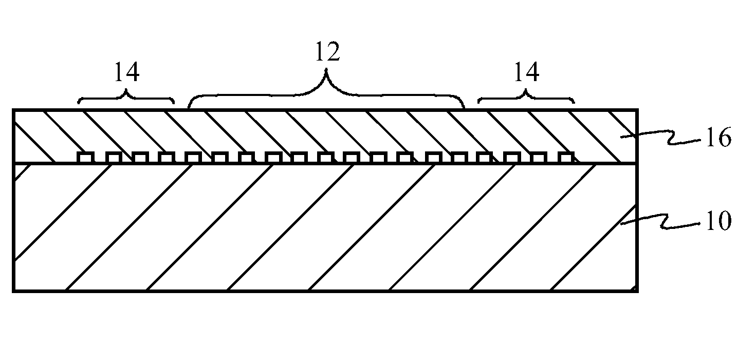
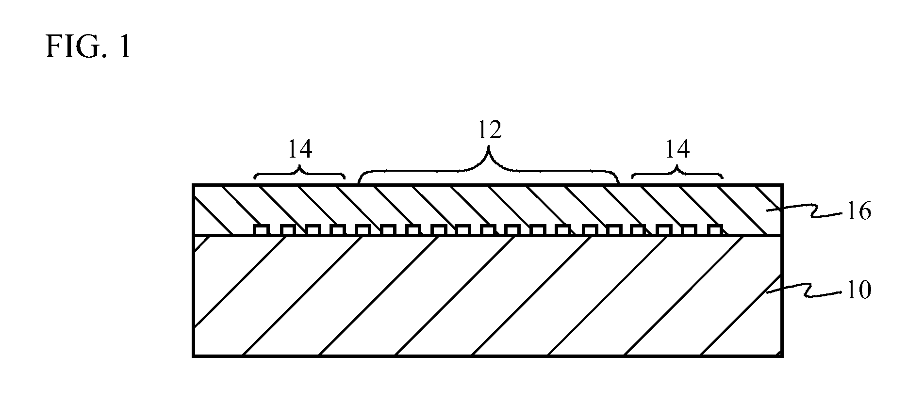
[0038]An acoustic wave device of a first embodiment is an exemplary resonator in an acoustic wave device with a comb-shaped electrode located on a piezoelectric substrate, and can be used in surface acoustic wave devices, Love wave devices, and boundary acoustic wave devices for example. FIG. 5A is a top view of the acoustic wave device in accordance with the first embodiment, and FIG. 5B is a cross-sectional view taken along line A-A in FIG. 5A. As illustrated in FIG. 5A, reflectors 24 are located at both sides of a comb-shaped electrode 22. The comb-shaped electrode 22 is an electrode that excites the acoustic wave, and in which two electrodes for input and output face each other so that respective electrode fingers are arranged alternately. The comb-shaped electrode 22 and the reflectors 24 mainly include Cu. As illustrated in FIG. 5B, the comb-shaped electrode 22 and the reflectors 24 are formed on a piezoelectric substrate 20 made of a 0-degree rotation Y-cut LN substrate. An F...

second embodiment

[0055]An acoustic wave device in accordance with a second embodiment is an exemplary resonator in an FBAR device. FIG. 11 is a cross-sectional view of the acoustic wave device of the second embodiment. As illustrated in FIG. 11, a lower electrode 32 made of, for example, Cu is located on a substrate 30 made of Si (silicon) for example. A piezoelectric film 34 made of, for example, AlN (aluminum nitride) is located on the lower electrode 32. An upper electrode 36 made of, for example, Cu is located on the piezoelectric film 34 so as to have a portion (resonance portion) that faces the lower electrode 32 across the piezoelectric film 34. An F-doped silicon oxide film 38 is located between the piezoelectric film 34 and the upper electrode 36 and in a region in which the lower electrode 32 and the upper electrode 36 face each other. A space 40 is located in the substrate 30 in the region in which the lower electrode 32 and the upper electrode 36 face each other.

[0056]In the FBAR device,...


PUM


Abstract

An acoustic wave device includes: an electrode that excites an acoustic wave and is located on a substrate; and a silicon oxide film that is located so as to cover the electrode and is doped with an element or molecule displacing O in a Si—O bond, wherein the element or molecule is F, H, CH3, CH2, Cl, C, N, P, or S.

Description

CROSS-REFERENCE TO RELATED APPLICATION[0001]This application is a continuation application of PCT / JP2011 / 060316 filed Apr. 27, 2011, the contents of which are herein wholly incorporated by reference.FIELD[0002]A certain aspect of the present invention relates to an acoustic wave device.BACKGROUND[0003]There has been known a surface acoustic wave device, which includes a comb-shaped electrode formed of IDTs (Interdigital Transducer) formed on a surface of a piezoelectric substrate, an FBAR (Film Bulk Acoustic Resonator) device, in which a lower electrode, a piezoelectric film, and an upper electrode are stacked on a substrate, and a Lamb wave device, in which a lower electrode, a piezoelectric film, and an upper comb-shaped electrode are stacked, as acoustic wave devices using acoustic waves. These acoustic wave devices are small and light, can obtain high attenuation, and thus are used as filters of wireless devices such as mobile phone terminals.[0004]Recent advancements in high pe...

Claims


Application Information

Patent Timeline
Patent Type & Authority Patents(United States)
IPC IPC(8): H03H9/02
CPCH01L41/047H03H9/02102H03H9/02834H03H9/131H03H9/174H10N30/87
Inventor MATSUDA, SATORUMATSUDA, TAKASHIMIURA, MICHIO
Owner TAIYO YUDEN KK
Why Eureka
Try Eureka