Process for producing capacitive electromechanical conversion device, and capacitive electromechanical conversion device
a technology of capacitive electromechanical and conversion device, which is applied in the direction of electrical transducers, mechanical vibration separation, beacon systems using ultrasonic/sonic/infrasonic waves, etc., can solve the problems of reducing productivity, changing the state of the bonded interface, and difficulty in finer arrangement of elements in an array, so as to reduce the poor bonding at the bonded interface in producing a capacitive electromechanical conversion device.
- Summary
- Abstract
- Description
- Claims
- Application Information
AI Technical Summary
Benefits of technology
Problems solved by technology
Method used
Image
Examples
example 1
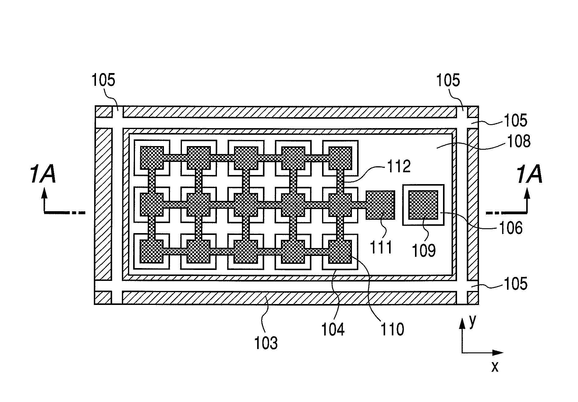
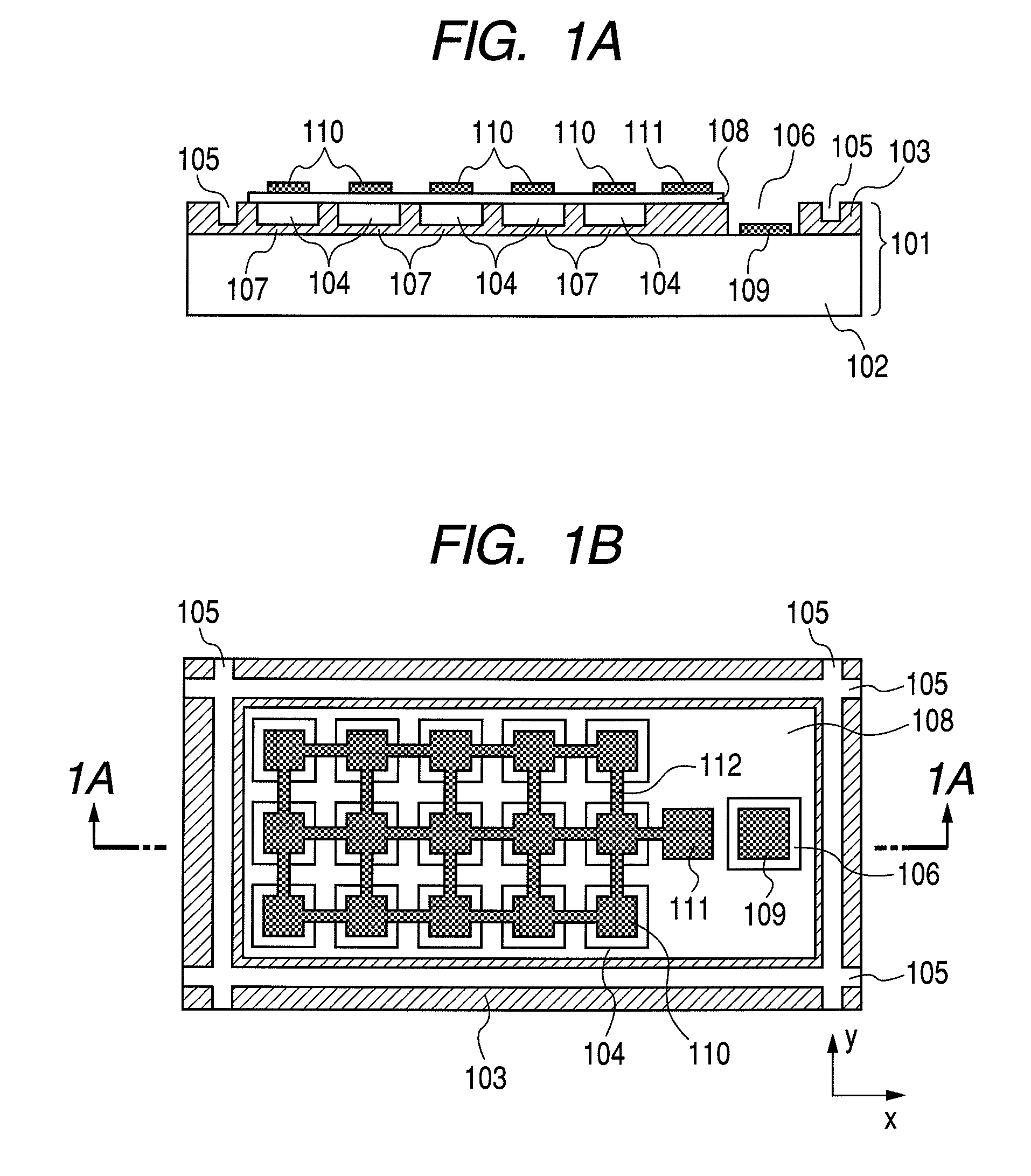
[0046]FIGS. 1A and 1B are a sectional view and a plan view, respectively, illustrating Example 1 relating to the capacitive electromechanical conversion device of the present invention. The same location has the same reference number. The sectional view of FIG. 1A corresponds to the 1A-1A location of FIG. 1B. In the present Example, a substrate 101 includes a silicon single-crystal layer 102, and a silicon oxide film layer 103 formed on the top surface thereof. The silicon single-crystal layer 102 is a substrate for the capacitive electromechanical conversion device, is electrically conductive, and also functions as an electrode. In the silicon oxide film layer 103, cavities (depressed portions) 104, grooves 105 as gas release paths, an electrode extraction portion 106, and electrically insulating layers 107 are formed. In addition, a membrane member 108 is bonded to the silicon oxide film layer 103. The membrane member 108 on the whole is in thin film, the portions formed above the...
example 2
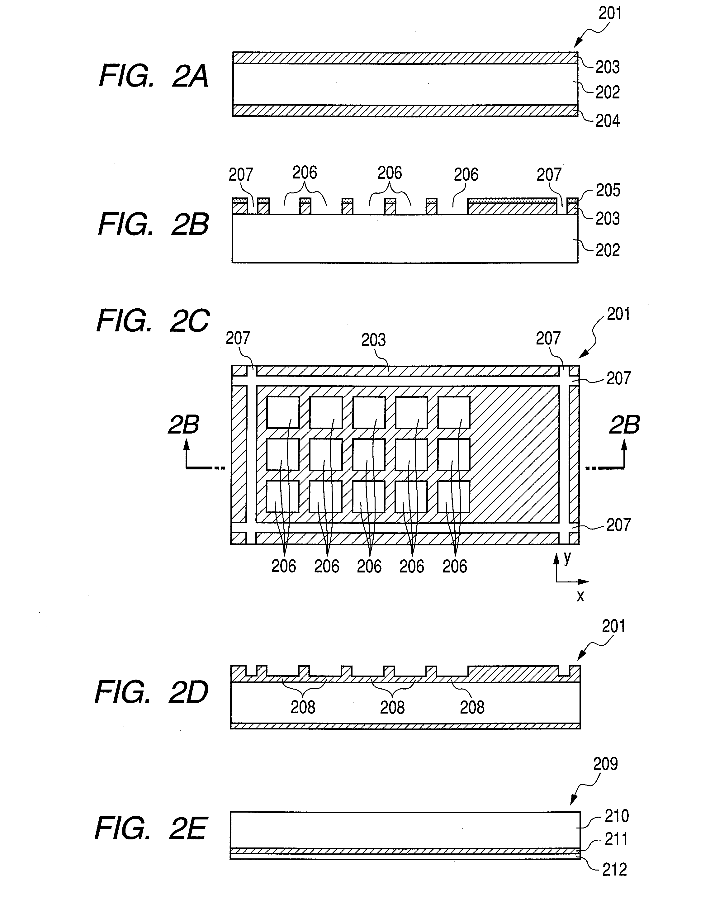
[0063]FIGS. 4A to 4Q are diagrams illustrating Example 2 relating to a process for producing the capacitive electromechanical conversion device of the present invention. The same location has the same reference number. The production process of the present Example begins at a substrate 401, a sectional view of which is illustrated in FIG. 4A. The substrate 401 includes a silicon single-crystal layer 402, and a silicon oxide film layer 403 and a silicon oxide film layer 404 formed on the top and bottom surface thereof, respectively.
[0064]First, as illustrated in FIG. 4B, a photoresist layer 405 is used as an etching resist and a silicon oxide film layer 403 is etched to form cavities (depressed portions) 406. If a hydrofluoric acid is used for etching, a silicon single-crystal layer 402 functions as an etch stop layer, making it easy to control the amount of etching in the depth direction. FIG. 4C illustrates a plan view of the cavities 406 seen from the silicon oxide film layer 403 ...
example 3
[0074]FIGS. 6A to 6H are diagrams illustrating Example 3 relating to a process for producing the capacitive electromechanical conversion device of the present invention. The same location has the same reference number.
[0075]The substrate 401 illustrated in FIG. 6A is the substrate in the same step as in FIG. 4D. In addition, the substrate illustrated in FIG. 6B is an SOI wafer 408, equivalent to that in FIG. 4E, that has a structure where a handle layer 409 comprising a silicon single crystal, a buried oxide film layer 410 comprising silicon oxide, and a device layer 411 comprising a silicon single crystal are laminated together in this order. In the present Example, as illustrated in FIG. 6C, a plurality of pores 601 is formed in the SOI wafer 408 so that the pores penetrate vertically through the wafer. The pores 601 function as gas release pores in a subsequent step. For example, deep reactive ion etching (DRIE) is suitable for processing the pores 601. In DRIE, for example, SF6 ...
PUM
| Property | Measurement | Unit |
|---|---|---|
| pressure | aaaaa | aaaaa |
| electrical conductivity | aaaaa | aaaaa |
| electrically insulating | aaaaa | aaaaa |
Abstract
Description
Claims
Application Information


