Array substrate and chip bonding method

a chip bonding and array substrate technology, applied in the field of display, can solve the problems contrast difference, glass mura (cog mura), etc., and achieve the effect of reducing the distance between the chip on the second output terminal group and the edge of the array substrate, ensuring display quality, and reducing the probability of poor chip bonding

Active Publication Date: 2021-08-24
WUHAN CHINA STAR OPTOELECTRONICS TECH CO LTD
View PDF9 Cites 0 Cited by
  • Summary
  • Abstract
  • Description
  • Claims
  • Application Information

AI Technical Summary

Benefits of technology

[0006]The object of the present invention is to provide an array substrate, able to reduce poor chip bonding and ensure display quality.
[0007]Another object of the present invention is to provide a chip bonding method, able to reduce poor chip bonding and ensure display quality.
[0024]The present invention provides the following advantages: the present invention provides an array substrate, the array substrate comprising: an active area, and a bonding area located around the active area, wherein the bonding area is provided with an input terminal group, a first output terminal group and a second output terminal a group; the first output terminal group is located at a side of the input terminal group away from the active area, and the second output terminal group is located between the first output terminal group and the input terminal group; when bonding chips, the first output terminal group or the second output terminal group being selected to cooperate with the input terminal group for chip bonding according to the type of the chip. As such, the distance between the chip on the second output terminal group and the edge of the array substrate is reduced when bonding the chip, the probability of poor chip bonding is also reduced and display quality is ensured. The present invention also provides a chip bonding method, capable of reducing poor chip bonding and ensuring display quality.

Problems solved by technology

Chip on glass mura (COG mura) is currently an important quality problem for LCD panels.
The reason why the chip is poorly bonded is that when the ACF is cured at a high temperature, the high temperature causes the chip and the thin film transistor (TFT) to also expand, thereby causing the uneven portion of the cell gap near the chip, leading to contrast difference when displaying.
At present, it is known that the distance from the edge of the chip to the edge of the array substrate is one of the main factors affecting the poor bonding of the chip.
The chip not integrated with RAM, which is smaller in size and more widely applied, is also very close to the edge of the array substrate, resulting in a high probability of poor chip bonding.

Method used


Image

  • Array substrate and chip bonding method
  • Array substrate and chip bonding method
  • Array substrate and chip bonding method

Examples


Embodiment Construction

[0035]To further explain the technical means and effect of the present invention, the following refers to embodiments and drawings for detailed description.

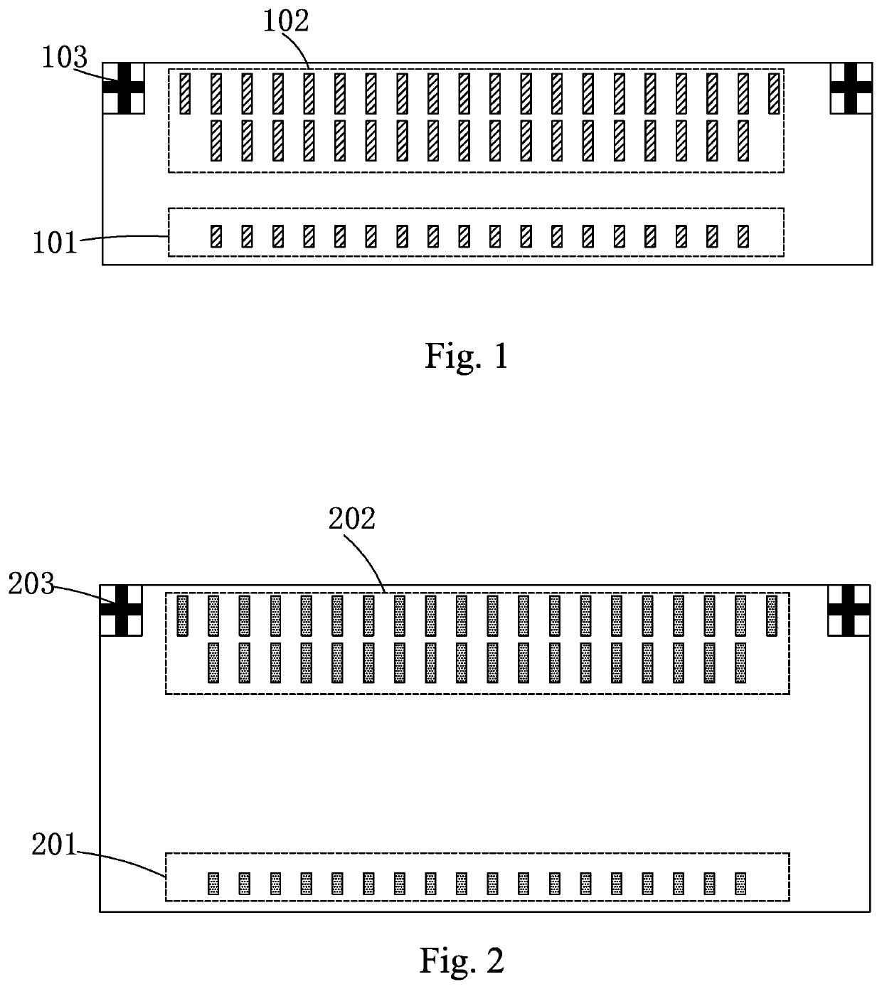
[0036]Refer to FIG. 6. The present invention provides an array substrate, comprising: an active area 10, a bonding area 20 located around the active area 10, wherein the bonding area 20 being provided with an input terminal group 21, a first output terminal group 22 and a second output terminal group 23;

[0037]the first output terminal group 22 being located at a side of the input terminal group 21 away from the active area 10, and the second output terminal group 23 being located between the first output terminal group 22 and the input terminal group 21; in other words, the first output terminal group 22, the second output terminal group 23 and the input terminal group 21 are sequentially disposed from top to bottom, and the distance to the edge of the array substrate is also gradually increasing.

[0038]When bonding chips, the fir...


PUM

PropertyMeasurementUnit
bonding areaaaaaaaaaaa
areaaaaaaaaaaa
sizeaaaaaaaaaa

Abstract

The invention provides an array substrate and chip bonding method, the array substrate comprising: an active area, and a bonding area located around the active area, wherein the bonding area is provided with an input terminal group, a first output terminal group and a second output terminal a group; the first output terminal group is located at a side of the input terminal group away from the active area, and the second output terminal group is located between the first output terminal group and the input terminal group; when bonding chips, the first output terminal group or the second output terminal group is selected to cooperate with the input terminal group for chip bonding according to the chip type. By simultaneously providing the first and second output terminal groups, the bonding of the second type chip increases the distance between the chip and the edge of the array substrate.

Description

BACKGROUND OF THE INVENTION1. Field of the Invention[0001]The present invention relates to the field of display, and in particular to an array substrate and chip bonding method.2. The Related Arts[0002]With the development of display technology, the panel display devices such as liquid crystal displays (LCDs), due to the advantages of high image quality, power saving, thinness and wide application range, are widely applied to various consumer electronic products, such as, mobile phones, televisions, personal digital assistants (PDA), digital cameras, notebook computers, and desktop computers, and have become mainstream in display devices.[0003]Chip on glass mura (COG mura) is currently an important quality problem for LCD panels. The existing chip bonding process includes: attaching an anisotropic conductive film (ACF) to a surface of the array substrate, and then placing the chip on a predetermined bonding position on the array substrate, and finally using a thermal head to press t...

Claims


Application Information

Patent Timeline
Patent Type & Authority Patents(United States)
IPC IPC(8): H01L23/00H01L27/12H01L25/18H01L25/00G02F1/1345H01L23/544
CPCH01L24/06H01L24/83H01L25/18H01L25/50H01L27/124G02F1/13458H01L23/544H01L2223/54426H01L2224/06155H01L2224/06177H01L2224/8313H01L2224/83851H05K1/18G02F1/133H01L2223/54486H01L2223/54473H01L2223/5442G02F1/13452H01L23/49838H01L24/81H01L2224/81132H01L2224/83132H01L2224/81903H01L2224/83203H01L2224/16227H01L2224/81191H01L2224/32225H01L24/16H01L24/32H01L2924/00014
Inventor GUO, CHUNPENGWANG, YINGCHIHUANG, CHUNHUNG
Owner WUHAN CHINA STAR OPTOELECTRONICS TECH CO LTD
Why Eureka
Try Eureka