Fringe field switching liquid crystal display device and method of fabricating the same
a liquid crystal display and fringe field technology, applied in semiconductor devices, instruments, electrical devices, etc., can solve the problem of contact hole formation of undercut within the pad portion, and achieve the effect of improving undercut and consumption
- Summary
- Abstract
- Description
- Claims
- Application Information
AI Technical Summary
Benefits of technology
Problems solved by technology
Method used
Image

Examples
first embodiment
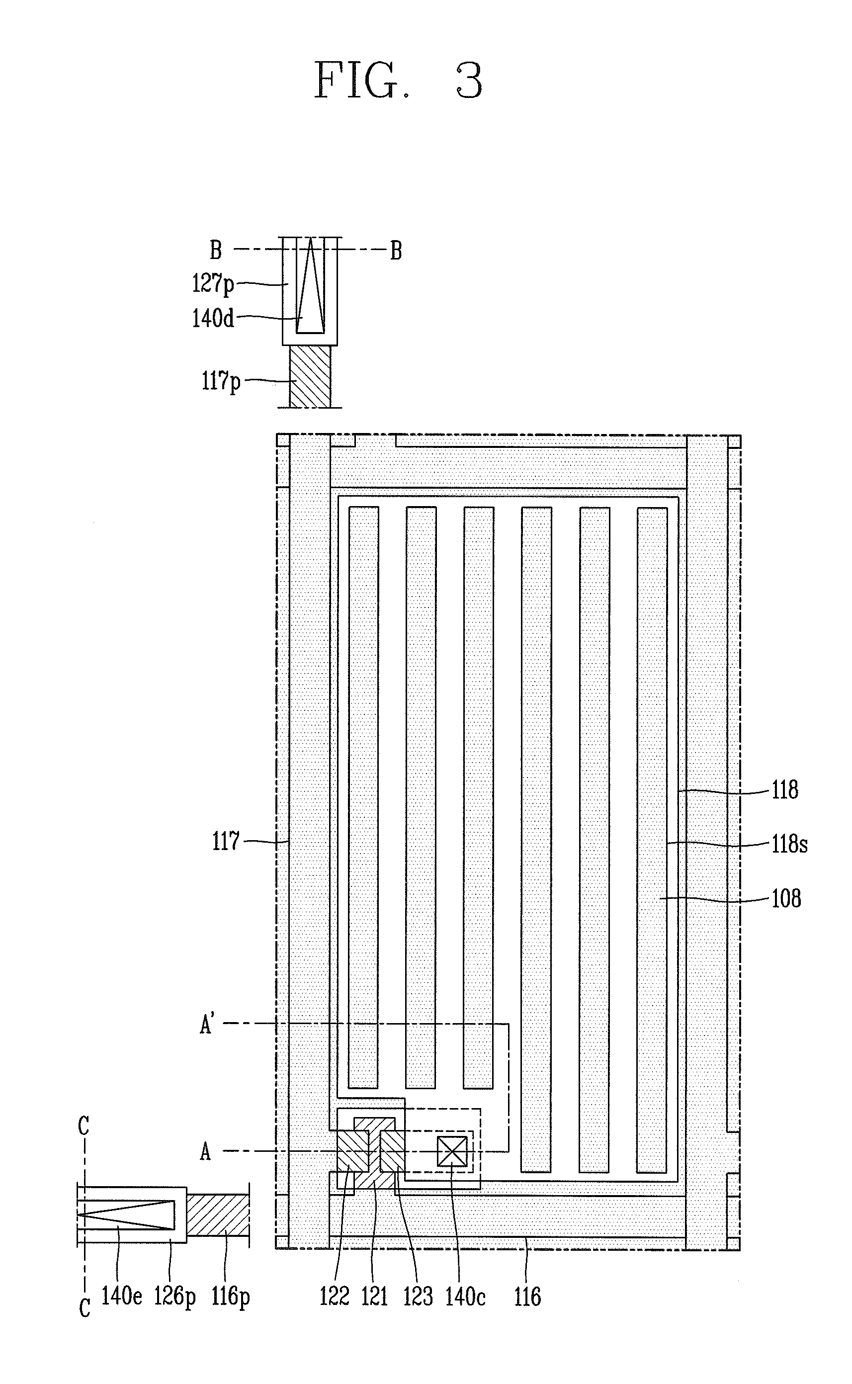
[0066]FIG. 3 is a schematic plan view showing a portion of an array substrate of an FFS LCD device according to the present invention, in which an image is displayed as a fringe field formed between a pixel electrode and a common electrode drives liquid crystal molecules positioned in a pixel region and on a pixel electrode through slits.
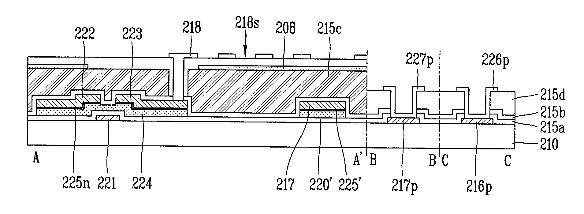
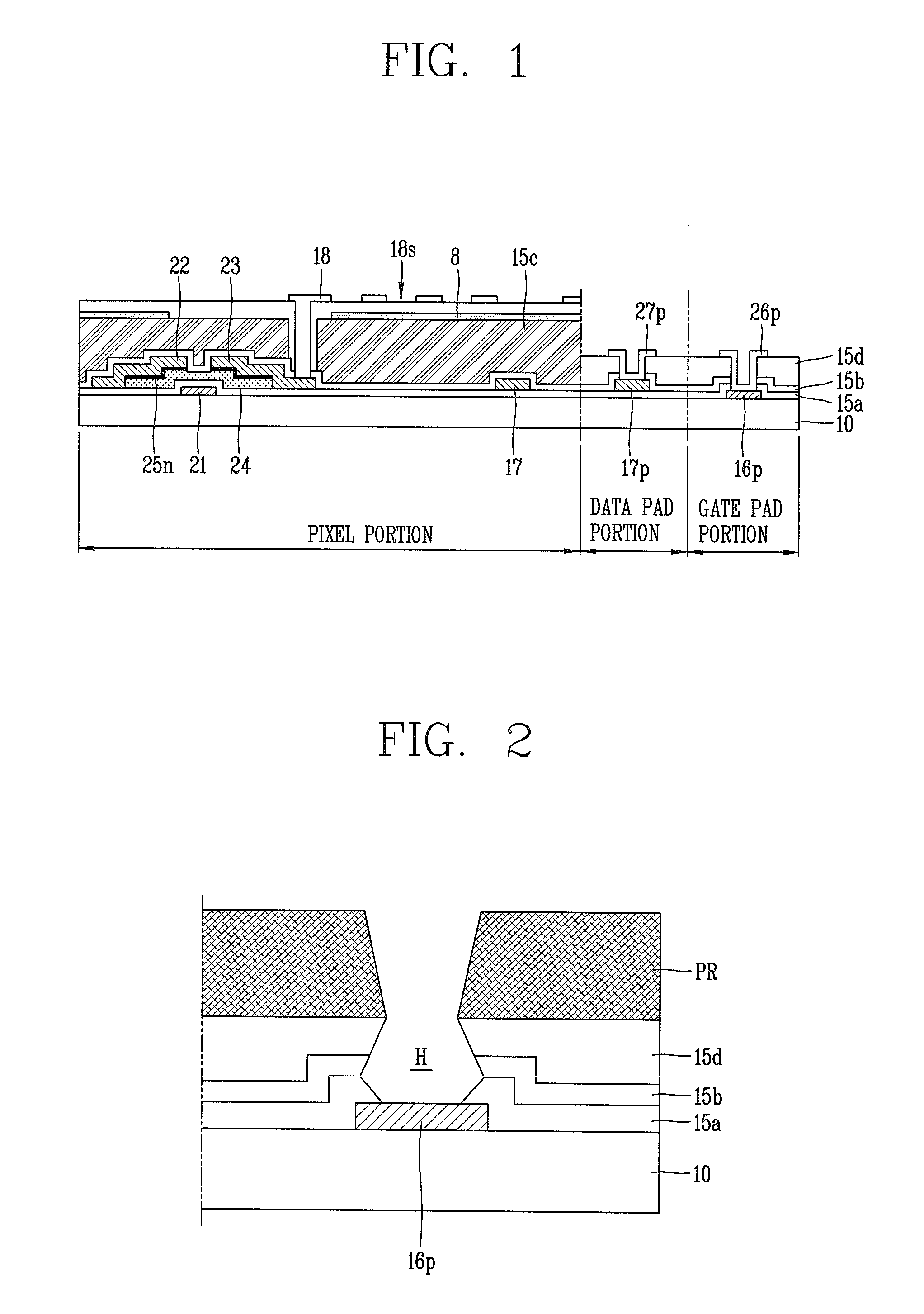
[0067]Also, FIG. 4 is a schematic sectional view showing a portion of the array substrate of the FFS LCD device according to the first embodiment of the present invention, taken along lines A-A′, B-B, and C-C of the array substrate illustrated in FIG. 3.
[0068]Here, a single pixel including a pixel portion, a data pad portion, and a gate pad portion is illustrated for description purpose. N number of gate lines and M number of data lines intersect to create M×N number of pixels exist in an actual LCD device. For the sake of explanation, a single pixel is illustrated in the drawings.
[0069]As illustrated in the drawings, a gate line 116 and a data line...
second embodiment
[0111]FIG. 7 is a schematic plan view illustrating a portion of an array substrate of an FFS LCD device according to the present invention.
[0112]FIG. 8 is a schematic sectional view illustrating a portion of the array substrate of the FFS LCD device according to the second embodiment of the present invention, taken along lines A-A′, B-B, and C-C of the array substrate illustrated in FIG. 7.
[0113]Here, as mentioned above, single pixel including a pixel portion, a data pad portion, and a gate pad portion is illustrated for description purpose. N number of gate lines and M number of data lines intersect so M×N number of pixels exist in an actual LCD device. But for the sake of explanation, a single pixel is illustrated in the drawings.
[0114]As illustrated in the drawings, a gate line 216 and a data line 217 are formed to be arranged vertically and horizontally to define a pixel region on the array substrate 210 according to a first embodiment of the present invention. Also, a thin film...
third embodiment
[0167]FIG. 13 is a plan view schematically illustrating a portion of an array substrate of an FFS LCD device according to the present invention.
[0168]FIG. 14 is a sectional view schematically illustrating a portion of the array substrate of the FFS LCD device according to the third embodiment of the present invention, taken along lines A-A′, B-B, and C-C of the array substrate illustrated in FIG. 13.
[0169]As mentioned above, single pixel including a pixel portion, a data pad portion, and a gate pad portion is illustrated for description purpose. N number of gate lines and M number of data lines intersect so M×N number of pixels exist in an actual LCD device. But for the sake of explanation, a single pixel is illustrated in the drawings.
[0170]As illustrated in the drawings, a gate line 316 and a data line 317 are formed to be arranged vertically and horizontally to define a pixel region on the array substrate 310 according to a first embodiment of the present invention. Also, a thin ...
PUM
 Abstract
Description
Claims
Application Information
 - R&D
- Intellectual Property
- Life Sciences
- Materials
- Tech Scout
- Unparalleled Data Quality
- Higher Quality Content
- 60% Fewer Hallucinations
Browse by: Latest US Patents, China's latest patents, Technical Efficacy Thesaurus, Application Domain, Technology Topic, Popular Technical Reports.
© 2025 PatSnap. All rights reserved.Legal|Privacy policy|Modern Slavery Act Transparency Statement|Sitemap|About US| Contact US: help@patsnap.com