Liquid crystal display device and a method of manufacturing the same

a technology of liquid crystal display and manufacturing method, which is applied in the direction of instruments, computing, electric digital data processing, etc., can solve the problems of low mass productivity and increase in manufacturing processes, and achieve the effects of suppressing the increase in cost, simplifying the manufacturing process, and preventing the generation of low-temperature bubbles

Active Publication Date: 2014-03-25
JAPAN DISPLAY WEST
View PDF14 Cites 3 Cited by
  • Summary
  • Abstract
  • Description
  • Claims
  • Application Information

AI Technical Summary

Benefits of technology

[0022]In the structure described above, a cross-sectional area of the spacer on one side with respect to the step in a height direction of the spacer is relatively large, and a cross-sectional area of the spacer on the other hand with respect to the step is relatively small. The large cross-sectional area side can be made to function as a supporting body (spacer). On the other hand, it is possible to obtain such a cross-sectional area as to adjust a restoring force against low-temperature bubbles by using the smaller cross-sectional area. That is to say, it is possible to realize with the spacer structure that when a large external pressure is applied to the spacer, although the spacer is deformed to a certain extent, the spacer is not readily deformed any more, and the low-temperature bubbles are prevented from being generated. The reason for this is that since when the external pressure is released, the restoring force of the substrate depends on a coupling force of the portion having the smaller cross-sectional area, the coupling force of the portion having the smaller cross-sectional area can be optimized for prevention of the generation of the low-temperature bubbles.
[0026]According to the present invention, it is possible to either dissolve or relax the trade-off relationship between the supporting strength of the spacer, and the prevention of the generation of the low-temperature bubbles. In addition, it is possible to simplify the manufacturing process for the relaxation of the trade-off relationship, and it is also possible to suppress the increase in cost as much as possible.

Problems solved by technology

However, such spacers different in height from one another results in an increase in the number of processes in manufacturing, and are difficult in control, which results in the low mass productivity.

Method used


Image

  • Liquid crystal display device and a method of manufacturing the same
  • Liquid crystal display device and a method of manufacturing the same
  • Liquid crystal display device and a method of manufacturing the same

Examples


first embodiment

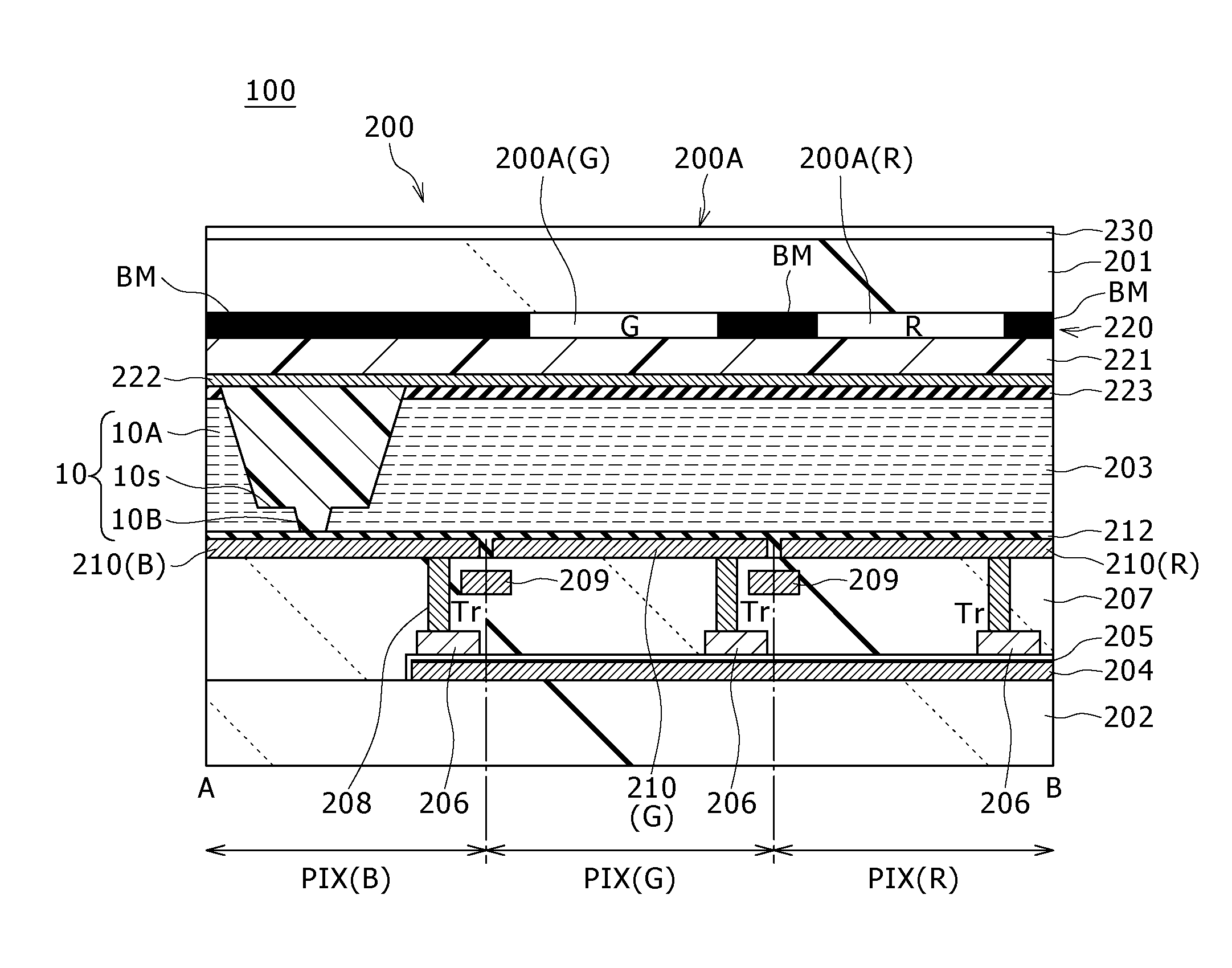
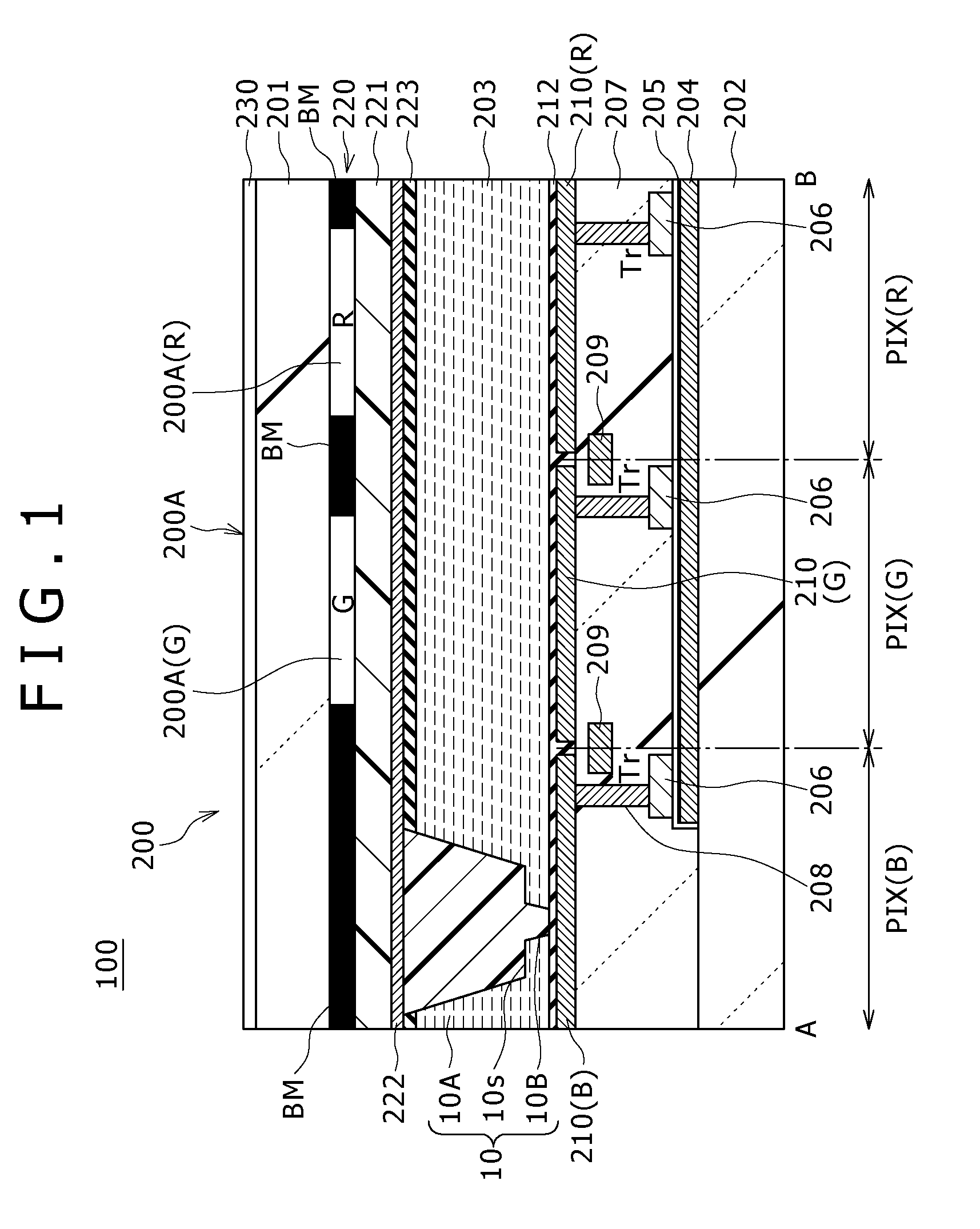
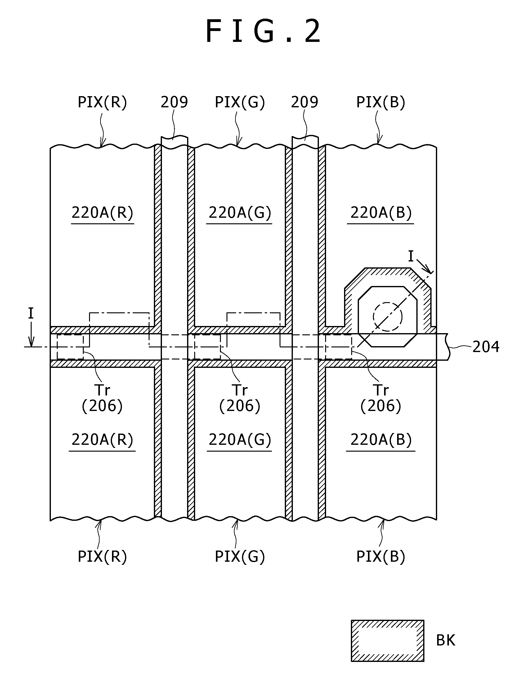
[0046]FIG. 1 is a schematic cross sectional view, showing a structure of a transmission type liquid crystal display device according to a first embodiment of the present invention, taken on line I-I of FIG. 2. FIG. 2 is a simplified plane transparent view showing a part of pixel areas which the transmission type liquid crystal display device of the first embodiment shown in FIG. 1 has.

[0047]The liquid crystal display device 100 illustrated in FIG. 1 has a liquid crystal panel 200, a backlight (not shown), and a drive portion (not shown) for driving the liquid crystal panel 200 and the backlight.

[0048]When viewed from the cross section shown in FIG. 1, in the liquid crystal panel 200, an upper side in FIG. 1 corresponds to “a display surface side,” and a lower side in FIG. 1 corresponds to “a back surface side.” The backlight is disposed on the back surface side so as to be close to the liquid crystal panel 200.

[0049]In the liquid crystal panel 200, a color filter substrate 201 as “a...

second embodiment

[0113]FIGS. 6A to 6E respectively show cross sectional views of the color filter substrate 201 when the spacer 10 having the multiple step structure in a transmission type liquid crystal display device according to the second embodiment of the present invention is manufactured.

[0114]As shown in FIG. 6A, the color filter layer 220 is formed on the color filter substrate 201, and the planarizing film 221 is formed on the color filter layer 220.

[0115]A first level negative resist NR1 is formed on the planarizing film 221 to have a predetermined thickness. Next, as shown in FIG. 6B, by using a photo mask for exposing a portion in which the spacer is intended to be formed of the negative resist NR1 thus formed, and light-blocking the periphery thereof, a negative resist NR portion of the portion in which the spacer is intended to be formed is exposed. As a result, a latent image corresponding to an opening pattern of the photo mask is formed within the negative resist NR1.

[0116]When the ...

third embodiment

[0123]FIGS. 7A and 7E respectively show cross sectional views of the color filter substrate 201 when the spacer 10 having the multiple step structure in a transmission type liquid crystal display device according to the third embodiment of the present invention is manufactured.

[0124]As shown in FIG. 6A, the color filter layer 220 is formed on the color filter substrate 201, and the planarizing film 221 is formed on the color filter layer 220.

[0125]A first level positive resist PR3 is formed on the planarizing film 221 to have a predetermined thickness. Next, as shown in FIG. 7B, by using a photo mask for light-blocking a portion in which the spacer is intended to be formed of the positive resist PR3 thus formed, and exposing the periphery thereof, there is exposed the periphery of a positive resist PR3 portion of the portion in which the spacer is intended to be formed is exposed. As a result, a latent image corresponding to a light-blocking pattern of the photo mask is formed withi...


PUM

PropertyMeasurementUnit
heights Hbaaaaaaaaaa

Abstract

Disclosed herein is a liquid crystal display device, including: a first substrate; a second substrate; a plurality of spacers disposed between the first substrate and the second substrate; and a liquid crystal layer filled between the first substrate and the second substrate supported by the plurality of spacers; wherein each of the plurality of spacers has a multiple step structure having one or more steps.

Description

BACKGROUND OF THE INVENTION[0001]1. Field of the Invention[0002]The present invention relates to a liquid crystal display device having a spacer for holding a gap with which a liquid crystal is enclosed between two sheets of substrates referred to as so-called a drive substrate and a counter substrate, respectively, and a method of manufacturing the same.[0003]2. Description of the Related Art[0004]A liquid crystal display device has advantages such as thinning, lightweight, and low power consumption. For this reason, many liquid crystal display devices are used in electronic apparatuses for mobile applications such as a mobile phone and a digital camera.[0005]The liquid crystal display device has a liquid crystal panel in which a liquid crystal is enclosed between a pair of substrates. With the liquid crystal display device, the liquid crystal panel modulates a light radiated from a flat surface light source such as a backlight provided on a back surface of the liquid crystal panel...

Claims


Application Information

Patent Timeline
Patent Type & Authority Patents(United States)
IPC IPC(8): G02F1/1339
CPCG02F1/133371G02F1/133504G06F3/0412G02F1/133512G02F2001/13396G02F2001/13398G02F1/133707G02F1/13394G02F1/13338G06F3/045G02F1/133555G02F1/13396G02F1/13398
Inventor KOITO, TAKEOTANAKA, TSUTOMUKOSAKA, HIDEHIRO
Owner JAPAN DISPLAY WEST
Why Eureka
Try Eureka