
Schottky junction source/drain transistor and method of making

a technology lateral growth, which is applied in the direction of basic electric elements, electrical equipment, semiconductor devices, etc., can solve the problems of degrading the performance of semiconductor chips, increasing the parasitic resistance of mosfet source/drain transistor, and increasing the length of mosfet channels, so as to achieve controllable and suppressed lateral growth

Inactive Publication Date: 2014-04-15
FUDAN UNIV
View PDF15 Cites 0 Cited by
  • Summary
  • Abstract
  • Description
  • Claims
  • Application Information

AI Technical Summary

Benefits of technology

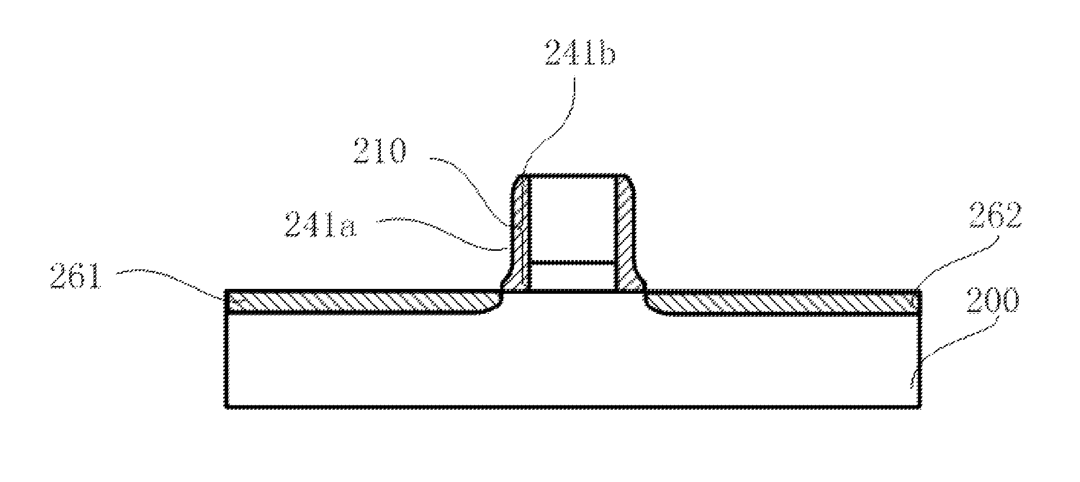
The present invention provides a method for making transistors that can form a Schottky junction with a ultra-thin and uniform vertical dimension, while controlling and suppressing lateral growth. This is achieved by using a material that can react with the metal layer during the annealing process, which prevents metal from diffusing towards the semiconductor layer. The resulting transistors have ultra-thin and uniform Schottky junctions with controllable and suppressed lateral growth.

Problems solved by technology

As the degree of integration of semiconductor chips continually increases, however, MOSFET channel length becomes shorter and shorter.
When the MOSFET channel length becomes very short, short-channel effect can degrade the performance of semiconductor chips, causing them to even malfunction.
The more and more shallow source / drain junction depths, however, together with limitations on dopant solid solubility, result in MOSFET source / drain parasitic resistance to become greater and greater, placing more and more demand on source / drain metal silicide (small-scale MOSFET typically use nickel silicide).
These requirements pose various challenges for the metallization processes at source / drain regions of nano-scale devices.
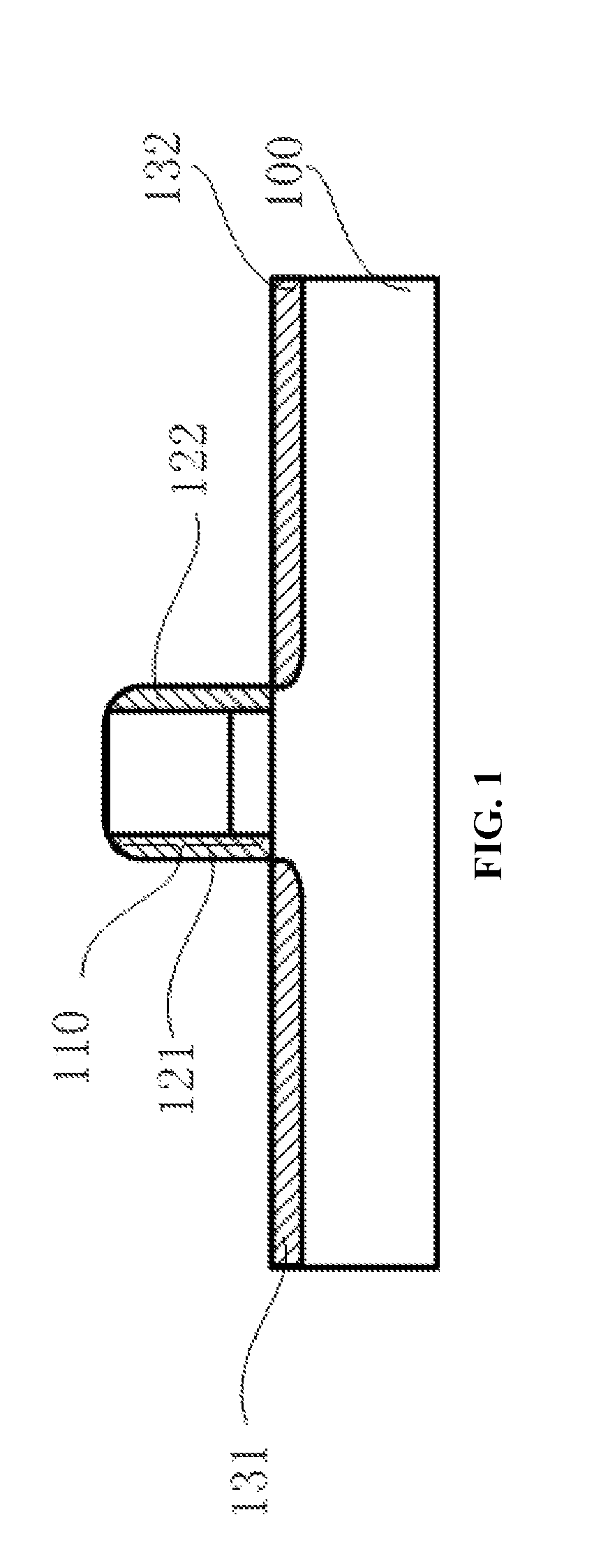
This leads to the formed nickel silicide to have uncontrollable and non-uniform thickness, and excessive lateral growth under the gate electrode 110, resulting in shortened channel length, reduced transistor threshold voltage, and increased leakage current.
Therefore, how to form a nickel silicide layer with a ultra-thin and uniform vertical dimension, and controllable and suppressed lateral growth, is a key challenge for the future P-N junction source / drain or Schottky junction source / drain MOSFET fabrication processes.

Method used


Image

  • Schottky junction source/drain transistor and method of making
  • Schottky junction source/drain transistor and method of making
  • Schottky junction source/drain transistor and method of making

Examples


Embodiment Construction

[0018]A method of making a transistor according to embodiments of the present invention is described in detail below with reference to the drawings.

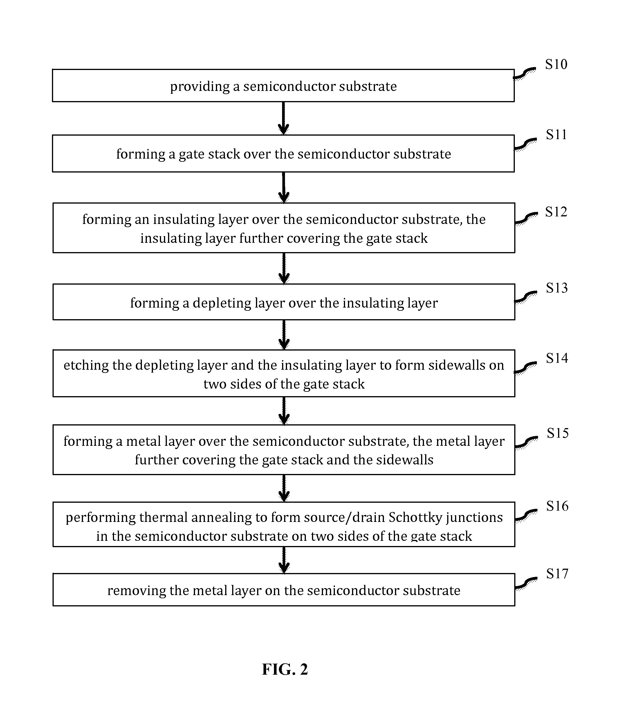
[0019]FIG. 2 is a flowchart illustrating a method for forming a Schottky junction source / drain transistor according to embodiments of the present invention. The method comprises: providing a semiconductor substrate (S10); forming a gate stack over the semiconductor substrate (S11); forming an insulating layer over the semiconductor substrate, the insulating layer further covering the gate stack (S12); forming a depleting layer over the insulating layer (S13); etching the depleting layer and the insulating layer to form composite sidewalls on two sides of the gate stack (S14); forming a metal layer over the semiconductor substrate, the metal layer further covering the gate stack and the sidewalls (S15); performing a thermal annealing process to form source / drain Schottky junctions in the semiconductor substrate on two sides of the gate st...


PUM

PropertyMeasurementUnit
temperatureaaaaaaaaaa
insulatoraaaaaaaaaa

Abstract

A method of making a transistor, comprising: providing a semiconductor substrate; forming a gate stack over the semiconductor substrate; forming an insulating layer over the semiconductor substrate; forming a depleting layer over the insulating layer; etching the depleting layer and the insulating layer; forming a metal layer over the semiconductor substrate; performing thermal annealing; and removing the metal layer. As advantages of the present invention, an upper outside part of each of the sidewalls include a material that can react with the metal layer, so that metal on two sides of the sidewalls is absorbed during the annealing process, preventing the metal from diffusing toward the semiconductor layer, and ensuring that the formed Schottky junctions can be ultra-thin and uniform, and have controllable and suppressed lateral growth.

Description

FIELD[0001]The present invention is related to semiconductor processing technologies, and more particularly to a Schottsky junction source / drain transistor and method of making.BACKGROUND[0002]With the development of semiconductor technologies, metal-oxide-semiconductor field-effect-transistors (MOSFET) have gained wide applications. In the recent years, microelectronics technologies around silicon integrated circuits have been rapidly developed. The degree of integration for semiconductor chips basically follows Moore's law, i.e., it increases by doubling every 18 months. As the degree of integration of semiconductor chips continually increases, however, MOSFET channel length becomes shorter and shorter. When the MOSFET channel length becomes very short, short-channel effect can degrade the performance of semiconductor chips, causing them to even malfunction.[0003]As the feature sizes of MOSFET devices continue to shrink, source / drain junction depths need to be more and more shallo...

Claims


Application Information

Patent Timeline
Patent Type & Authority Patents(United States)
IPC IPC(8): H01L21/336H01L21/338
CPCH01L29/66848H01L29/6653H01L29/7839
Inventor WU, DONGPINGLUO, JUNPIAO, YINGHUAZHU, ZHIWEIZHANG, SHILIZHANG, WEI
Owner FUDAN UNIV
Learn More