Object moving apparatus, object processing apparatus, exposure apparatus, object inspecting apparatus and device manufacturing method
a technology of object moving apparatus and processing apparatus, applied in the direction of conveyor parts, turning machine accessories, printers, etc., to achieve the effect of high accuracy
- Summary
- Abstract
- Description
- Claims
- Application Information
AI Technical Summary
Benefits of technology
Problems solved by technology
Method used
Image
Examples
first embodiment
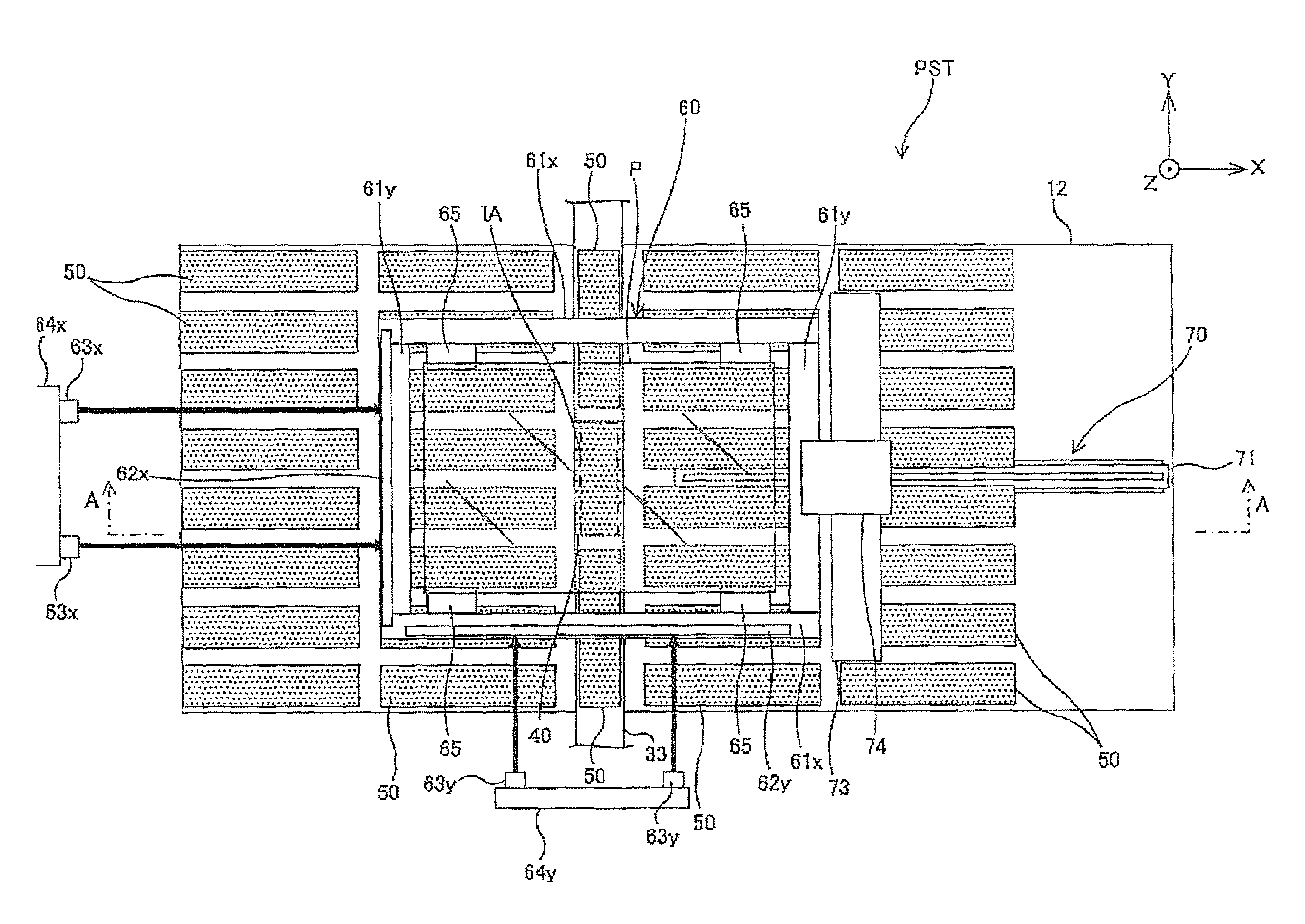
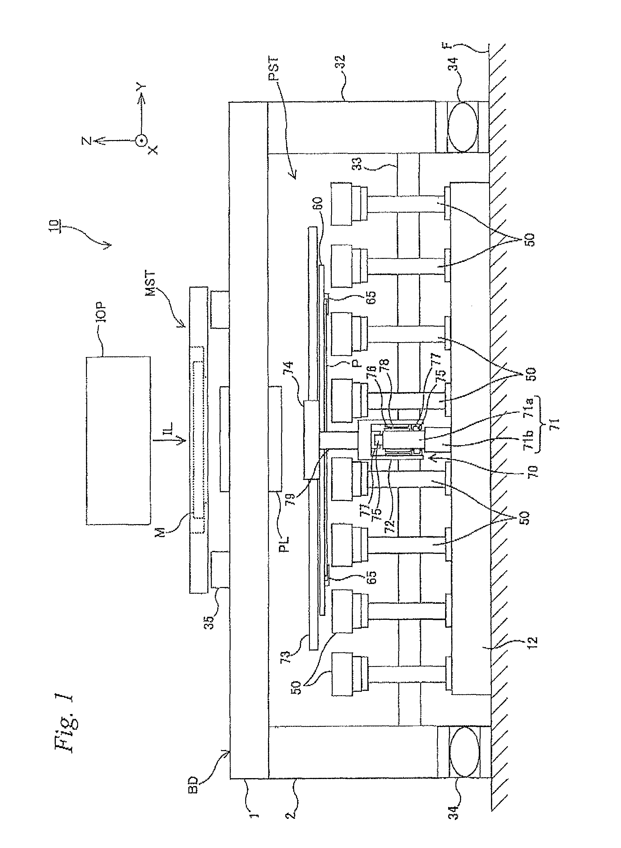
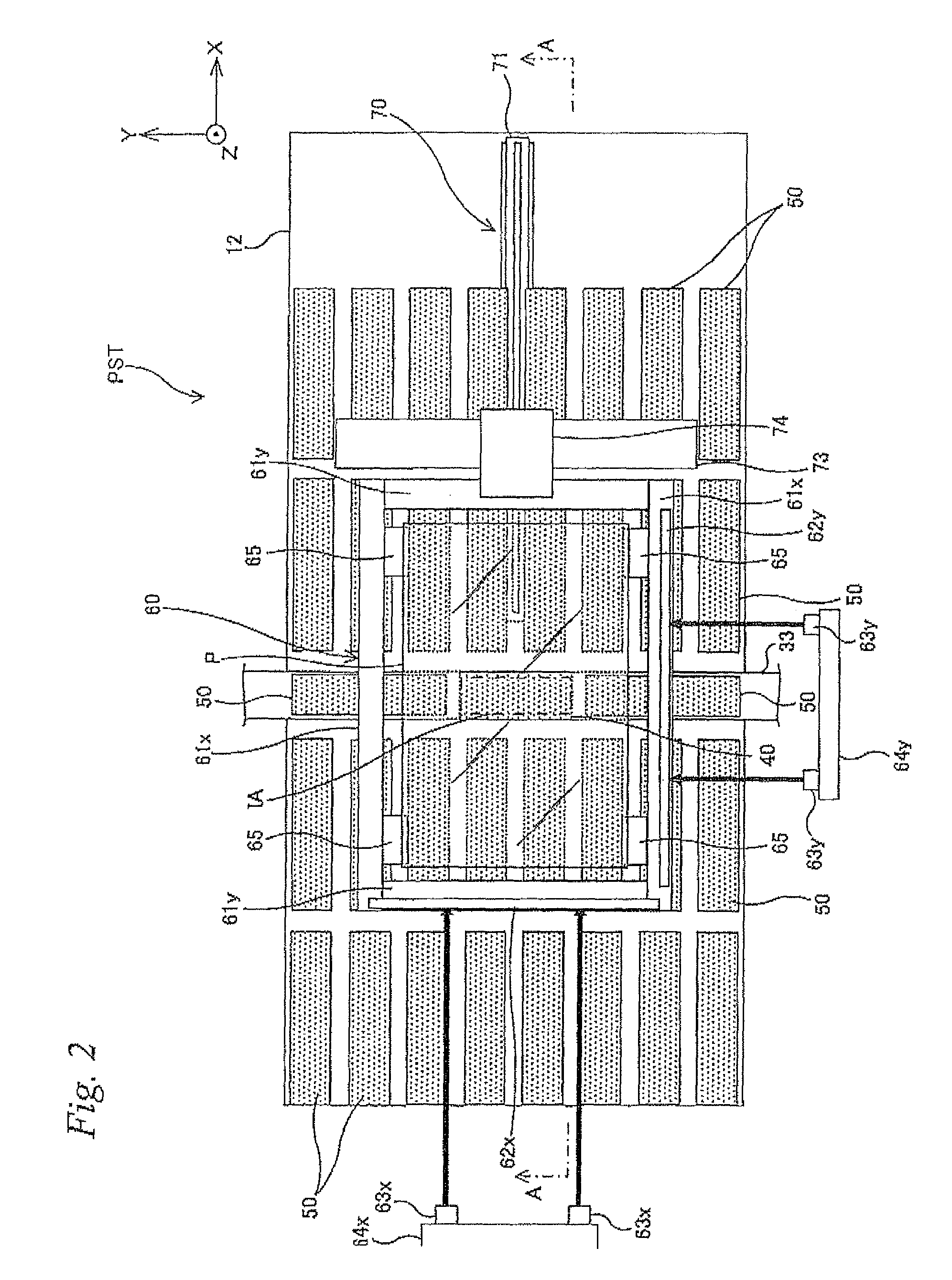
[0043]A first embodiment of the present invention is described below, with reference to FIGS. 1 to 6C.
[0044]FIG. 1 shows a schematic configuration of a liquid crystal exposure apparatus 10 related to the first embodiment that is used in manufacturing of flat-panel displays, for example, liquid crystal display devices (liquid crystal panels) or the like. Liquid crystal exposure apparatus 10 is a projection exposure apparatus by a step-and-scan method, in which a rectangular glass substrate P (hereinafter, simply referred to as a substrate P) that is used for a display panel of a liquid crystal display device serves as an exposure subject, which is a so-called scanner.
[0045]As shown in FIG. 1, liquid crystal exposure apparatus 10 is equipped with illumination system IOP, a mask stage MST that holds a mask M, a projection optical system PL, a body BD on which mask stage MST and projection optical system PL described above and the like are mounted, a substrate stage device PST that hold...
second embodiment
[0096]Next, a liquid crystal exposure apparatus of a second embodiment is described. Since the liquid crystal exposure apparatus of the present second embodiment has a configuration similar to the configuration of liquid crystal exposure apparatus 10 of the first embodiment described earlier except that a configuration of a substrate stage device that holds substrate P is different, only the configuration of the substrate stage device is explained in the description below. Herein, from the viewpoint of preventing the redundant description, members which have functions equivalent to those of the first embodiment are denoted by the same reference signs as the reference signs in the first embodiment and the description thereabout is omitted.
[0097]As shown in FIG. 7A, in a substrate stage device PST2 related to the second embodiment, a configuration of a substrate holding frame 260 is different from the first embodiment. The different points are explained below. Similarly to the first e...
third embodiment
[0102]Next, a third embodiment is described. Since a liquid crystal exposure apparatus of the third embodiment has a configuration similar to the configuration of each of the liquid crystal exposure apparatuses of the first and second embodiments described earlier except that a configuration of a substrate stage device that holds substrate P is different, only the configuration of the substrate stage device is described below. Incidentally, members which have functions similar to those in the first and second embodiments described above are denoted by the same reference signs as the reference signs in the first and second embodiments described above and the description thereabout is omitted.
[0103]As shown in FIG. 8, in a substrate stage device PST3 related to the present third embodiment, a drive unit 370 has a pair of X guides 71, which is different from the first embodiment described above. The pair of X guides 71 are placed parallel to each other at a predetermined distance in th...
PUM
| Property | Measurement | Unit |
|---|---|---|
| size | aaaaa | aaaaa |
| length | aaaaa | aaaaa |
| wavelength | aaaaa | aaaaa |
Abstract
Description
Claims
Application Information


