Inductor element, integrated circuit device, and three-dimensional circuit device

Active Publication Date: 2014-04-22
THRUCHIP JAPAN INC
View PDF25 Cites 12 Cited by
  • Summary
  • Abstract
  • Description
  • Claims
  • Application Information

AI Technical Summary

Benefits of technology

The present invention allows for wires to cross through the opening in a coil, which reduces the area of the circuit and simplifies the wiring. This results in fewer vias and wires needed, making the circuit more efficient.

Problems solved by technology

In order to compensate for this, high power is required, and a problem arises, such that the power consumption increases.
In this case also a problem arises, such that the efficiency of transmission is low when there are three or more semiconductor chips.
In the case where an electrical field passes through films having different dielectric constants, there is reflection in the interface, and thus the efficiency of signal transmission is low.
They confirmed that a peripheral wire running in one direction like conventional bus lines barely affect the efficiency of transmission.

Method used


Image

  • Inductor element, integrated circuit device, and three-dimensional circuit device
  • Inductor element, integrated circuit device, and three-dimensional circuit device
  • Inductor element, integrated circuit device, and three-dimensional circuit device

Examples


first embodiment

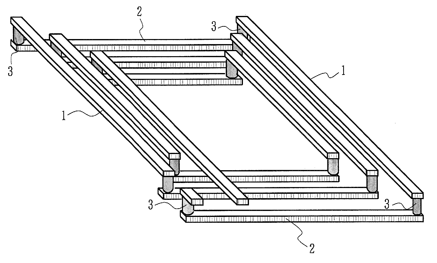
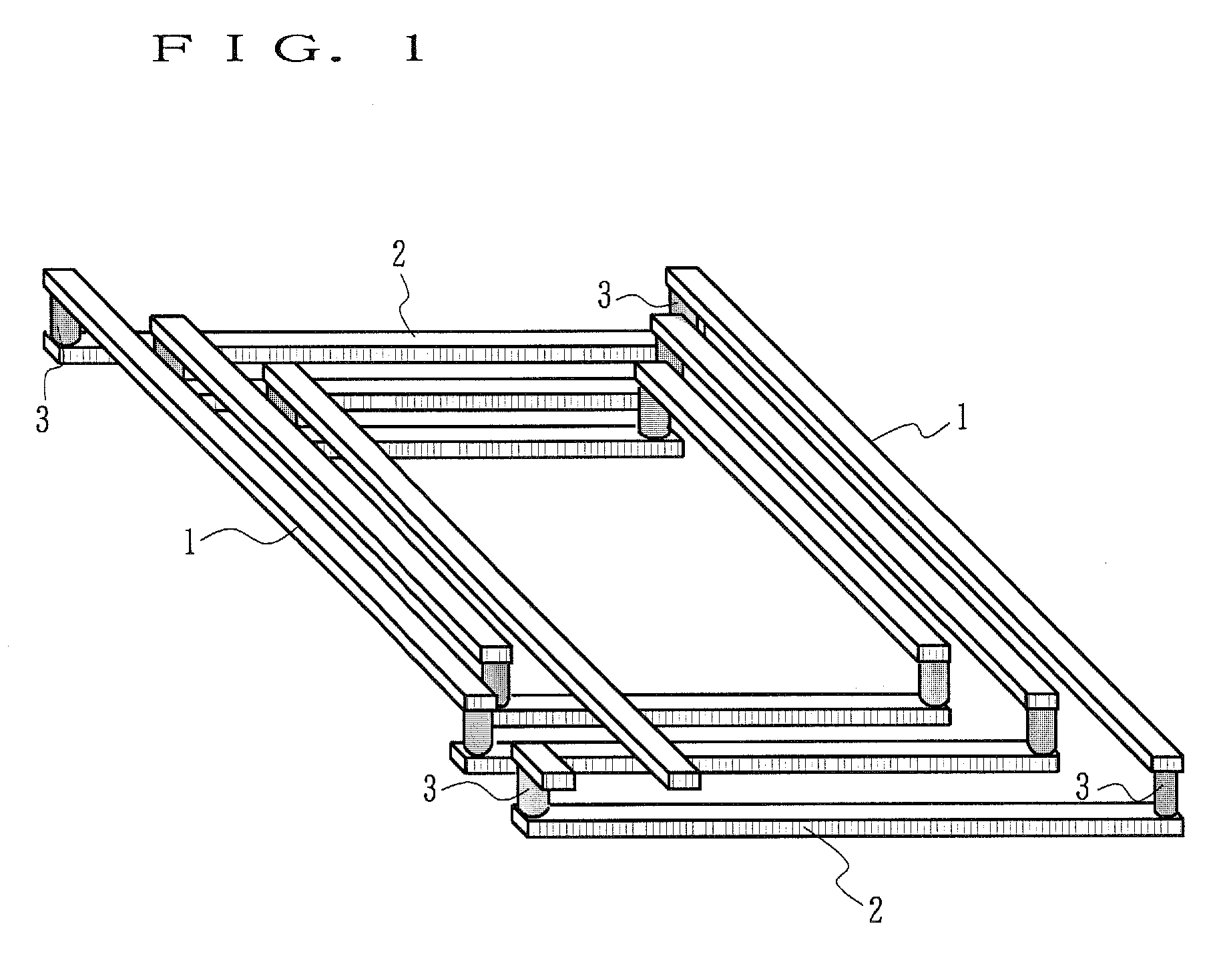
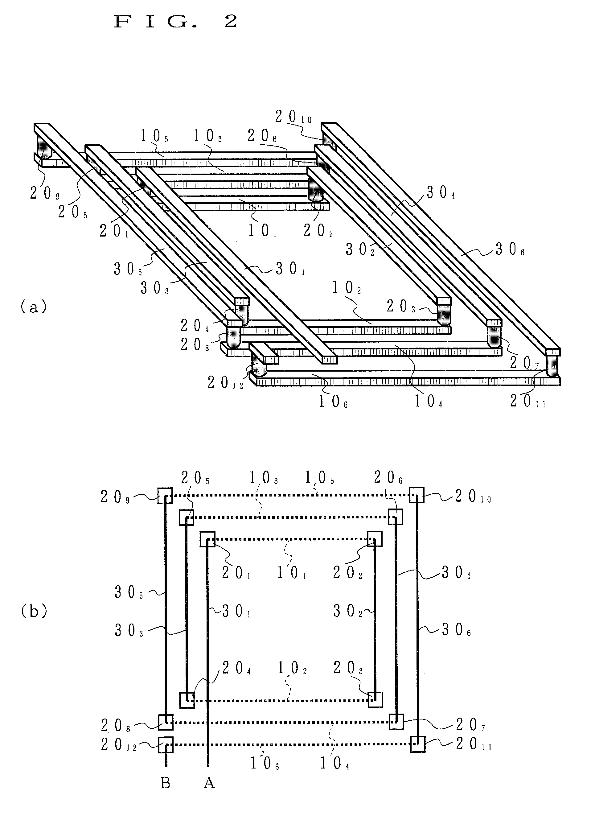
[0076]Taking the above into consideration, the inductor element according to the first embodiment of the present invention is described in reference to FIGS. 2 to 5.

[0077]FIGS. 2(a) and 2(b) are diagrams illustrating the structure of the inductor element according to the first embodiment of the present invention. FIG. 2(a) is a conceptual perspective diagram, and FIG. 2(b) is a conceptual projection plan diagram.

[0078]As shown in the figures, straight first coil elements 10 are formed of first layer metal wires and second coil elements 30 which run in a direction perpendicular to the first coil elements are formed of second layer metal wires, and the first coil elements 10 and the second coil elements 30 are alternately connected through connection vias 20 so that a single coil that winds clockwise is formed.

[0079]In this case the direction in which the coil elements are wired is the same as that in which main wires, for example bus lines, are wired in each layer.

[0080]Here, the coi...

second embodiment

[0101]Next, the inductor element according to the second embodiment of the present invention is described in reference to FIG. 6. The inductor element according to the second embodiment is different from that according to the first embodiment only in its pattern as seen from the top, and the basic manufacturing process is exactly the same, and therefore only the conceptual projection plan diagram is described.

[0102]FIG. 6 is a conceptual projection plan diagram showing the inductor element according to the second embodiment of the present invention, and the projection plan pattern is the same as that for the conventional inductor element in FIG. 10. In the present case, two leads are formed using second layer metal wires.

[0103]In the second embodiment, connection vias are formed in the corners of the rectangle, and therefore the first coil elements 108 and 1010 formed of first layer metal wires are bent, unlike in the above first embodiment, but the peripheral wires that cross the c...

third embodiment

[0105]Next, the inductor element according to the third embodiment of the present invention is described in reference to FIG. 7. The inductor element according to this embodiment is gained by layering two inductor elements as in the above first embodiment and connecting them.

[0106]FIG. 7(a) is a conceptual projection plan diagram showing the inductor element according to the third embodiment of the present invention, FIG. 7(b) is a schematic perspective diagram showing a corner, FIG. 7(c) is a schematic perspective diagram showing the portion that leads out from point B, and FIG. 7(d) is a conceptual perspective diagram showing the connection portion between two sub-coils.

[0107]Here, the coil elements 10, 30, 50 and 70 may be formed in a line and space pattern with a width of 1 μm, for example.

[0108]In the figure, the first coil elements 10 are the dotted lines, the second coil elements 30 are the solid lines, the third coil elements 50 are the one-dot chain lines, and the fourth co...


PUM


Abstract

The invention relates to an inductor element, an integrated circuit device and a three-dimensional circuit device where a wire passes through the opening of a coil so that the efficiency in the use of wires is high.Coil elements are provided in the main direction of wires in at least two adjacent layer levels having different main directions of wires, and the coil elements are connected to coil elements formed in different layer levels so that a single coil is formed.

Description

TECHNICAL FIELD[0001]The present invention relates to an inductor element, an integrated circuit device and a three-dimensional circuit device, and in particular, to an inductor element, an integrated circuit device and a three-dimensional circuit device characterized by their structure: an inductor element for communication between substrates like bare IC chips or printed circuit boards using magnetic coupling is formed without greatly affecting the arrangement of other wires on bare IC chips or printed circuit boards.BACKGROUND ART[0002]Together with the miniaturization of portable electronics in recent years, integrated semiconductor circuit devices have been required to be mounted with higher density. In order to make this possible, attempts have been made to stack a number of semiconductor chips three-dimensionally.[0003]In three-dimensional integrated semiconductor circuit devices, semiconductor chips are generally connected through micro-bumps so that signals can be exchanged...

Claims


Application Information

Patent Timeline
IPC IPC(8): H01F5/00
CPCH01L2225/06527H01F2017/002H01L2924/0002H01F17/0013H01L23/645H01L28/10H01L25/0657H01L23/5227H01L2924/00H01F5/00
Inventor KURODA, TADAHIRO
Owner THRUCHIP JAPAN INC
Why Eureka
Try Eureka