
Solid-state imager and signal processing system

a solid-state imager and signal processing technology, applied in the field of solid-state imager and signal processing system, can solve the problems that the disclosed technique cannot cope with the high-speed signal transmission requirement, and achieve the effect of reducing the electromagnetic noise generated in increasing the freedom of layout of the optical communication unit, and reducing the heat generated by the optical communication uni

Inactive Publication Date: 2014-04-22
SONY CORP
View PDF9 Cites 14 Cited by
  • Summary
  • Abstract
  • Description
  • Claims
  • Application Information

AI Technical Summary

Benefits of technology

[0008]It is thus desirable to provide a solid-state imager that transmits at a high speed a pixel signal read from a pixel unit in the form of light signal and controls the effect of heat attributed to optical communication and to provide a signal processing system including the solid-state imager.
[0012]According to embodiments of the present invention, the arrangement of the optical communication unit on the bottom surface of the substrate opposite the top surface bearing the pixel unit increases the freedom of layout of the optical communication unit. Since this arrangement allows the substrate to be interposed between the pixel unit and the optical communication unit, the effect of heat generated by the optical communication unit on the pixel unit is reduced. Also, the effect of the electromagnetic noise generated in the optical communication unit on the pixel unit is reduced.
[0013]The use of the signal line for transferring the signal read from the pixel unit to the optical communication unit on the bottom surface of the substrate increases the freedom of selection of the signal transfer method of the optical communication unit on the bottom surface of the substrate. For example, a signal transfer method is selected from a variety of signal transmission methods including a superimposition serial transmission method in which a synchronization signal is transmitted on a data line with a clock signal superimposed thereon, and a transmission method in which a plurality of clock signals are transmitted with serial data lines used.
[0014]The optical communication unit is manufactured in a manufacturing process different from a manufacturing process of the pixel unit. The integration of the optical communication unit is easy and the freedom of internal layout of the optical communication unit is thus increased.

Problems solved by technology

Japanese Unexamined Patent Application Publication No. 2006-196972 discloses only a structure in which a light emitter is mounted on a substrate having a solid-state imager and the disclosed technique is unable to cope with the high-speed signal transmission requirement.

Method used


Image

  • Solid-state imager and signal processing system
  • Solid-state imager and signal processing system
  • Solid-state imager and signal processing system

Examples


first embodiment

Structure of Solid-State Imager of First Embodiment

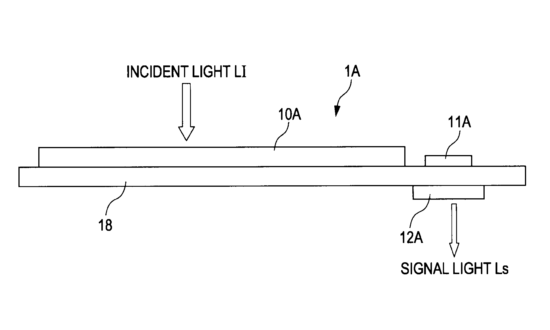
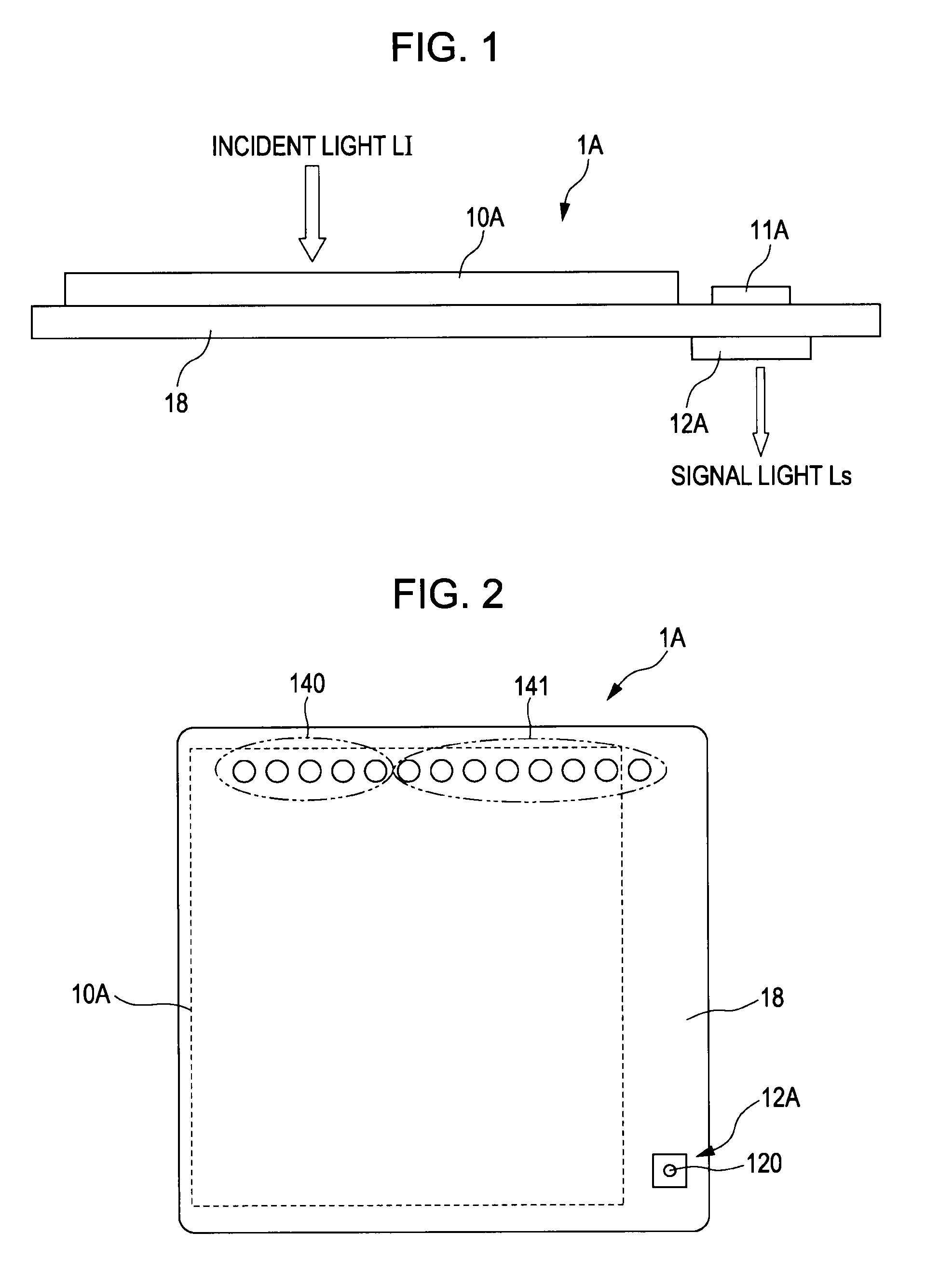
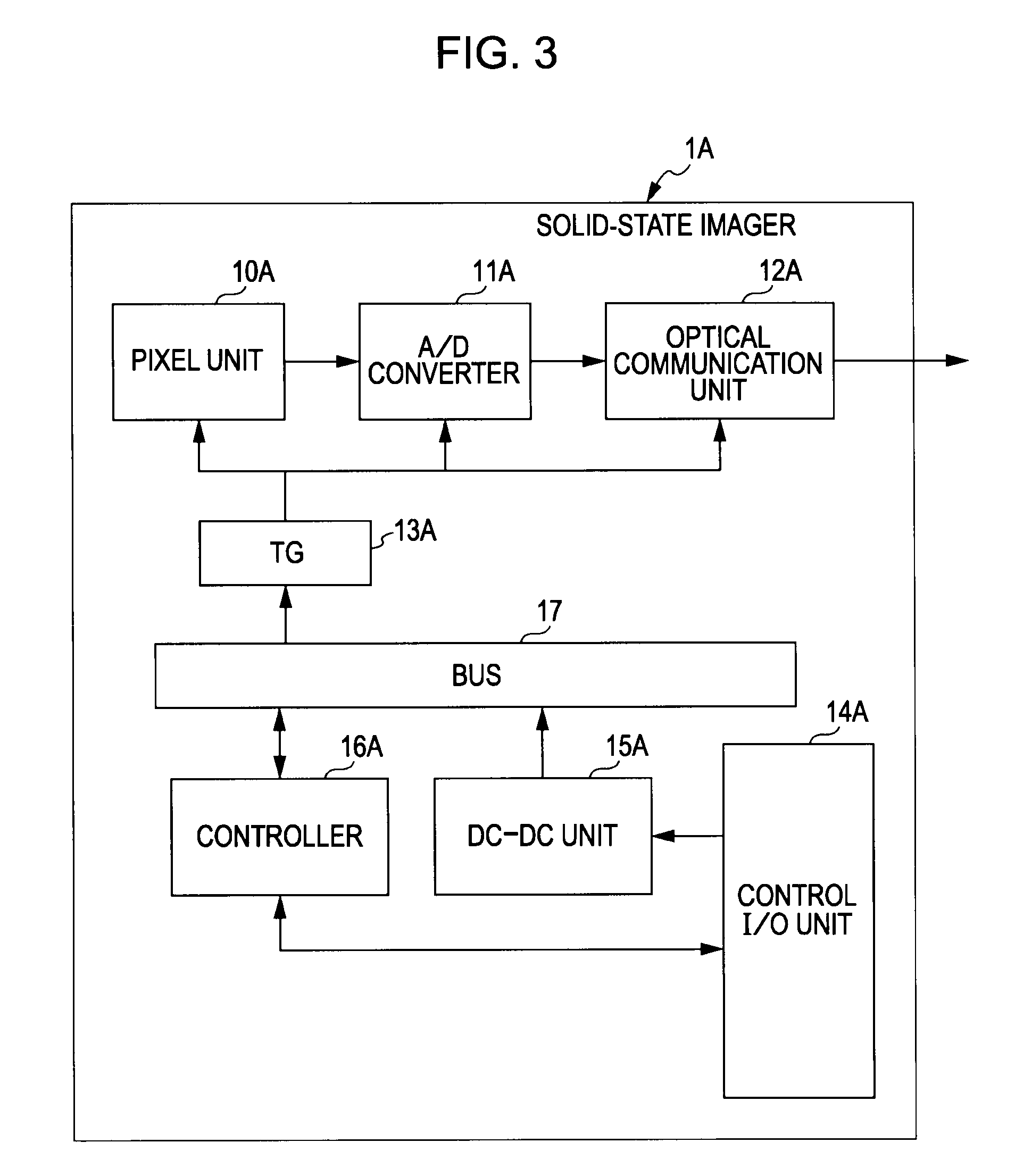
[0087]FIGS. 1 and 2 illustrate a solid-state imager 1A in accordance with a first embodiment of the present invention. FIG. 1 is a side view diagrammatically illustrating the solid-state imager 1A of the first embodiment, and FIG. 2 is a plan view diagrammatically illustrating the solid-state imager of the first embodiment. FIG. 3 is a functional block diagram illustrating a function of the solid-state imager 1A of the first embodiment.

[0088]The solid-state imager 1A of the first embodiment is a complementary metal oxide semiconductor (CMOS) image sensor or a charge-coupled device (CCD) image sensor. The solid-state imager 1A includes a pixel unit 10A converting light into an electrical signal and outputting the electrical signal. The pixel unit 10A includes one-dimensionally or two-dimensionally arranged pixels, each pixel converting light into the electrical signal, and thus outputs the electrical signal responsive to the intensit...

second embodiment

Structure of the Solid-State Imager of Second Embodiment

[0128]FIGS. 11 and 12 illustrate a solid-state imager 1B in accordance with a second embodiment of the present invention. FIG. 11 is a side view diagrammatically illustrating the solid-state imager 1B of the second embodiment, and FIG. 12 is a plan view diagrammatically illustrating the solid-state imager 1B of the second embodiment.

[0129]The solid-state imager 1B of the second embodiment includes a light blocker 200 and / or a cooler 201 on the optical communication unit 12A arranged on the bottom surface of the substrate 18 for the pixel unit 10A.

(1) One Example of the Solid-State Imager Having the Light Blocker

[0130]FIG. 13 is a side view diagrammatically illustrating the solid-state imager 1B having the light blocker 200, and FIG. 14 is a side view diagrammatically illustrating a comparative solid-state imager having no light block unit. The structure and operation of the solid-state imager 113 having the light blocker 200 on...


PUM


Abstract

A solid-state imager includes a pixel unit for converting incident light into an electrical signal, a substrate bearing the pixel unit formed thereon, an analog-to-digital converter, formed on the substrate, for converting a signal read from the pixel unit into a digital signal, an optical communication unit, arranged on the bottom surface of the substrate opposite the surface of the substrate bearing opposite the top surface of the substrate bearing the pixel unit receiving the incident light, for converting the digital signal converted by the analog-to-digital converter into a light signal and outputting the light signal, and a signal line for transferring the digital signal, converted by the analog-to-digital converter, to the optical communication unit arranged on the bottom surface of the substrate.

Description

BACKGROUND OF THE INVENTION[0001]1. Field of the Invention[0002]The present invention relates to a solid-state imager for converting an optical image into an electrical signal and a signal processing system including the solid-state imager. More specifically, the present invention relates to a signal processing system that outputs in the form of a light signal a pixel signal read from the solid-state imager.[0003]2. Description of the Related Art[0004]As the degree of integration and speed of operation of circuit boards are increased, a remedial step to the delaying of signals and the generation of electromagnetic interference (EMI) becomes an urgent necessity. Optical wiring technique currently draws attention. The optical wiring technique is free from signal delay and signal degradation caused by electric wiring and electromagnetic interference noise radiated from the electric wiring, and can transfer data at a high speed.[0005]Japanese Unexamined Patent Application Publication No...

Claims


Application Information

Patent Timeline
Patent Type & Authority Patents(United States)
IPC IPC(8): H04N5/378H04N5/374H01L27/15H04N5/335H04N5/357H04N5/372H04N3/14H01L27/146H04N5/369H04N5/225
CPCH04N5/378H01L27/14609H01L27/14643H04N5/3742H04N25/767H04N25/75
Inventor OGASAWARA, HIDEHIKOSEKIYA, TOSHIYUKI
Owner SONY CORP
Learn More