Functional component compensation reconfiguration system and method

a functional component and reconfiguration system technology, applied in the field of semiconductor/solid-state device testing/measurement, memory address/allocation/relocation, instruments, etc., can solve the problems of high cost, resource intensive activity, complex manufacturing process for building integrated circuits, etc., and achieve the effect of changing the operational characteristics of functional components

Active Publication Date: 2014-04-29
NVIDIA CORP
View PDF394 Cites 23 Cited by
  • Summary
  • Abstract
  • Description
  • Claims
  • Application Information

AI Technical Summary

Benefits of technology

[0013]The present invention systems and methods enable configuration of functional components in integrated circuits. A present invention system and method can flexibly change the operational characteristics of functional components in an integrated circuit based upon a variety of factors including manufacturing defects, compatibility characteristics, performance requirements,

Problems solved by technology

However, designing and building integrated circuits with diverse functionality and performance characteristics is challenging.
Additionally, the manufacturing process to build the integrated circuits is highly complex and resource intensive.
Manufacturing integrated circuits is an expensive, resource intensive activity, in which numerous computational components are included in a single integrated circuit unit.
However, providing appropriate and efficient functionality at acceptable reliability is often difficult.
Yields for wafers w

Method used


Image

  • Functional component compensation reconfiguration system and method
  • Functional component compensation reconfiguration system and method
  • Functional component compensation reconfiguration system and method

Examples


Embodiment Construction

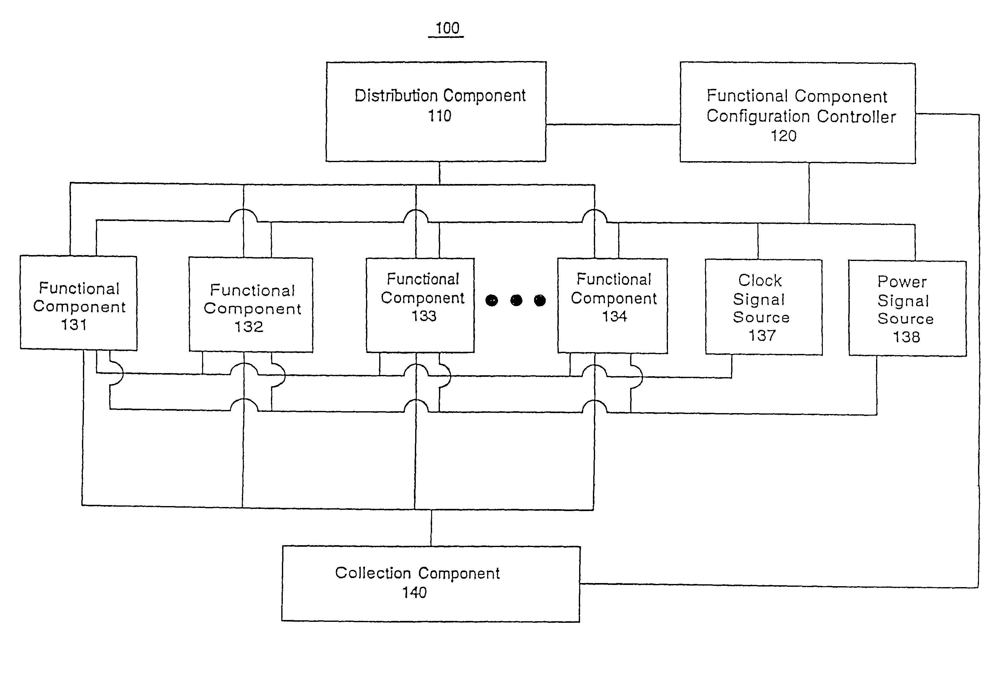
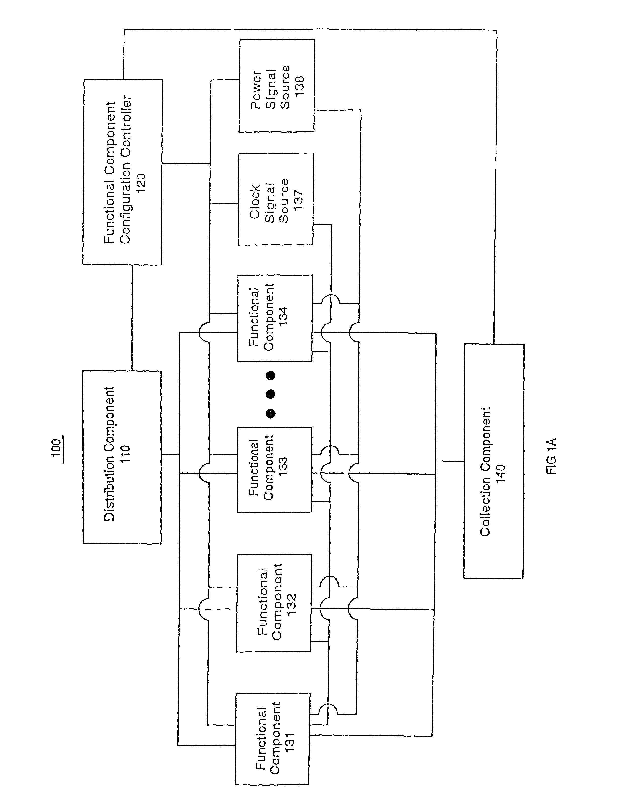
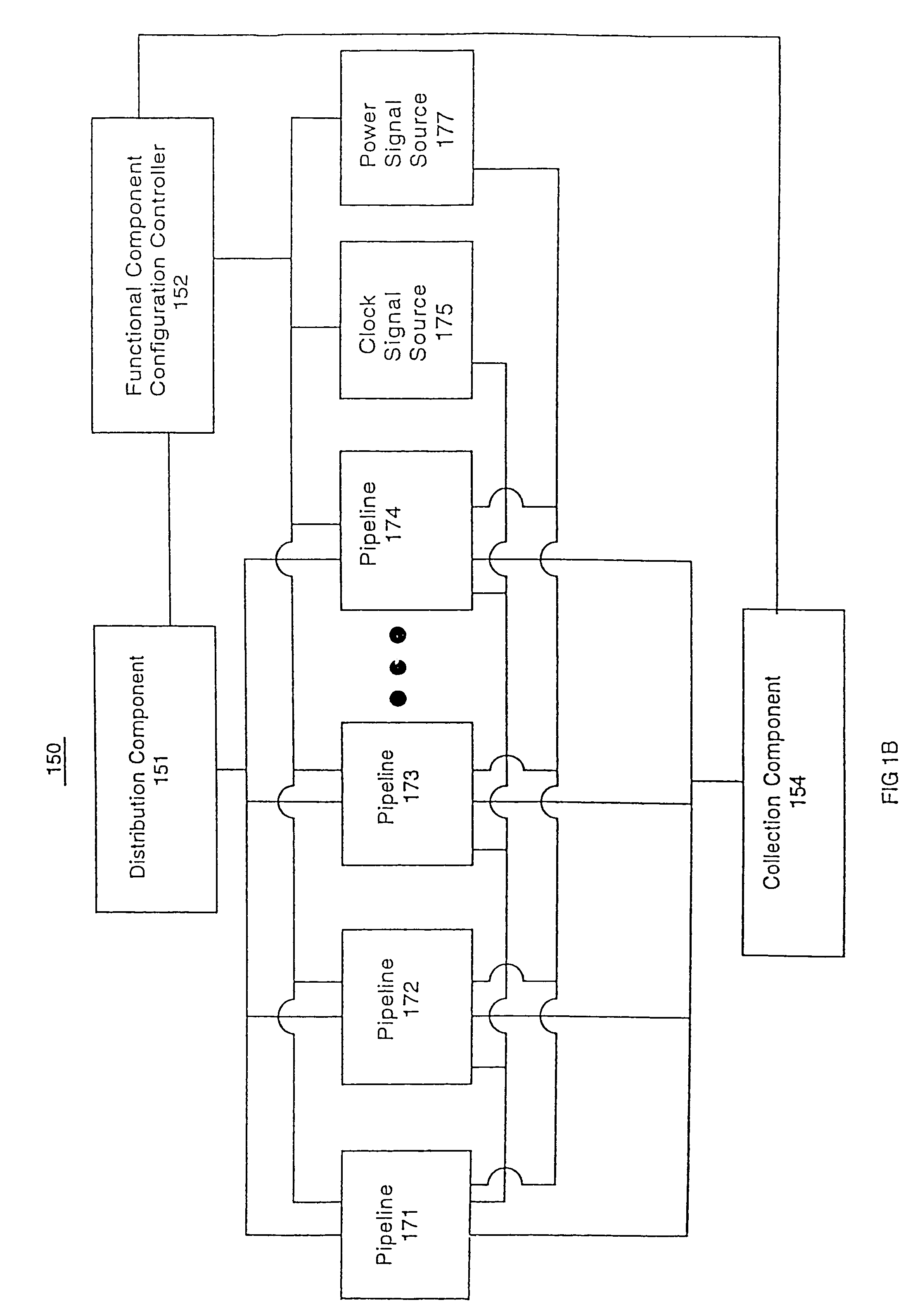
[0042]Reference will now be made in detail to the preferred embodiments of the invention, examples of which are illustrated in the accompanying drawings. While the invention will be described in conjunction with the preferred embodiments, it will be understood that they are not intended to limit the invention to these embodiments. On the contrary, the invention is intended to cover alternatives, modifications and equivalents, which may be included within the spirit and scope of the invention as defined by the appended claims. Furthermore, in the following detailed description of the present invention, numerous specific details are set forth in order to provide a thorough understanding of the present invention. However, it will be obvious to one of ordinary skill in the art that the present invention may be practiced without these specific details. In other instances, well known methods, procedures, components, and circuits have not been described in detail as not to unnecessarily ob...


PUM


Abstract

A memory cell reconfiguration process is performed in accordance with the operational characteristic settings determined based upon the results of analysis and/or testing of memory cell operations. The memory circuit can include a plurality of memory cells and memory cell configuration controller. The memory cells store information associated with a variety of operations. The memory cell configuration controller coordinates selective enablement and disablement of each of the plurality of memory cells, which can be done on a subset or group basis (e.g., enables and/or disables memory cells on a word length or row by row basis). The address mapping can be adjusted so that the memory space appears continuous to external components. The memory cell configuration controller can also forward configuration information to upstream and/or downstream components that can adjust operations to compensate for the memory cell configuration (e.g., to prevent overflow).

Description

RELATED APPLICATIONS[0001]This application is a continuation-in-part and claims the benefit of the following pending and commonly-owned U.S. patent applications:[0002]Patent application Ser. No. 10 / 740,721 filed Dec. 18, 2003, entitled “AN INTEGRATED CIRCUIT CONFIGURATION SYSTEM AND METHOD”;[0003]Patent application Ser. No. 10 / 740,722, filed Dec. 18, 2003, entitled “A SYSTEM AND METHOD FOR CONFIGURING SEMICONDUCTOR FUNCTIONAL CIRCUITS”;[0004]Patent application Ser. No. 10 / 740,723, filed Dec. 18, 2003, entitled “A SYSTEM AND METHOD FOR INCREASING DIE YIELD”;[0005]Patent application Ser. No. 10 / 740,779, filed Dec. 18, 2003, entitled “A SYSTEM AND METHOD FOR REMOTELY CONFIGURING SEMICONDUCTOR FUNCTIONAL CIRCUITS”; and[0006]Patent application Ser. No. 10 / 876,340, filed Jun. 23, 2004, entitled “A SYSTEM AND METHOD FOR TESTING AND CONFIGURING SEMICONDUCTOR CIRCUITS”; which are hereby incorporated by this reference.FIELD OF THE INVENTION[0007]The present invention relates to the field of s...

Claims


Application Information

Patent Timeline
IPC IPC(8): G06F12/10G09G5/39G06T9/00
CPCG06F11/267G11C29/56008G06F11/2289G06F11/1428G01R31/31704G11C2029/0409G11C29/00G01R31/318544G11C8/06G06F11/2035G01R31/3185H01L22/22G11C29/82
Inventor SCOTZNIOVSKY, STEFANCORY, BRUCEYOUNG, CHARLES CHEW-YUENTAMASI, ANTHONY M.VAN DYKE, JAMES M.MONTRYM, JOHN S.TREICHER, SEAN J.
Owner NVIDIA CORP
Why Eureka
Try Eureka