

Semiconductor radio frequency switch with body contact
a radio frequency switch and body contact technology, applied in the direction of semiconductor devices, electrical equipment, transistors, etc., can solve the problems of increasing the reducing power consumption, and reducing the off-state drain-to-source capacitance of each fet element. , to achieve the effect of improving linearity performance, reducing the off-state drain-to-source capacitance of each fet element, and reducing
- Summary
- Abstract
- Description
- Claims
- Application Information
AI Technical Summary
Benefits of technology
Problems solved by technology
Method used
Image

Examples
Embodiment Construction
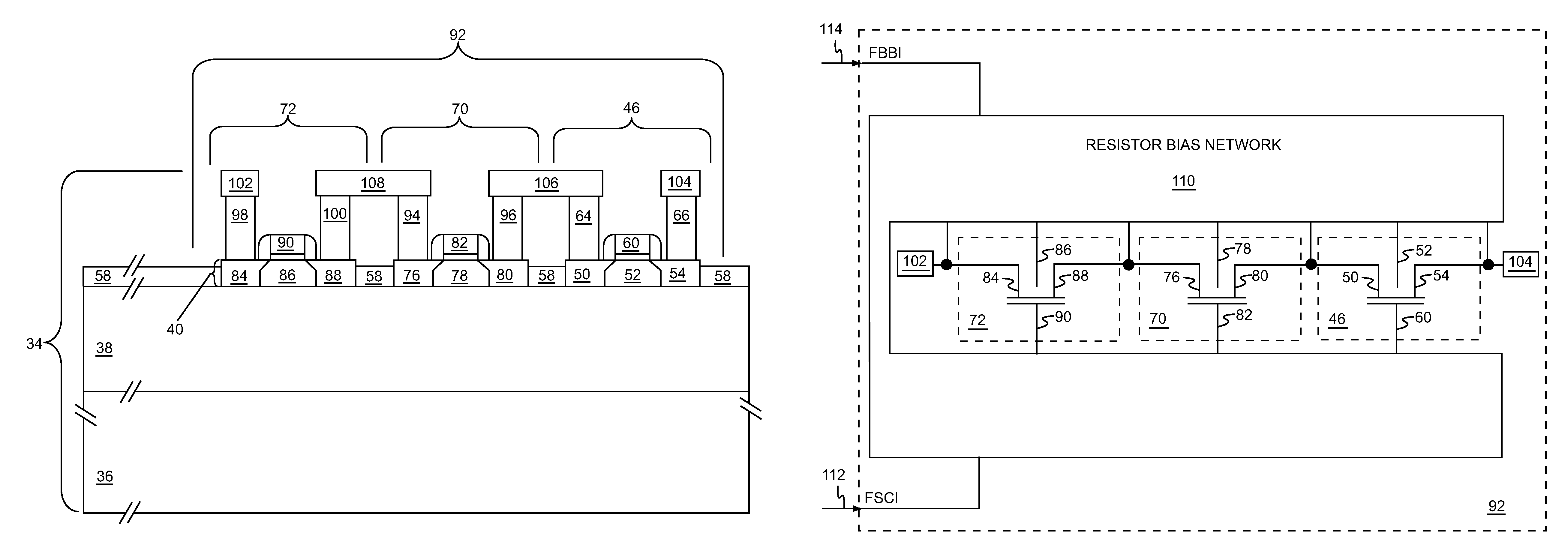
[0005]The present disclosure relates to an RF switch that includes multiple body-contacted field effect transistor (FET) elements coupled in series. The FET elements may be formed using a thin-film semiconductor device layer, which is part of a thin-film semiconductor die. Conduction paths between the FET elements through the thin-film semiconductor device layer and through a substrate of the thin-film semiconductor die may be substantially eliminated by using insulating materials. Elimination of the conduction paths allows an RF signal across the RF switch to be divided across the series coupled FET elements, such that each FET element is subjected to only a portion of the RF signal. Further, each FET element is body-contacted and may receive reverse body biasing when the RF switch is in an OFF state, thereby reducing an OFF state drain-to-source capacitance of each FET element. The combination of dividing the RF signal and reverse body biasing each FET element when the RF switch i...
PUM
 Abstract
Description
Claims
Application Information