
Semiconductor devices and methods of assembling same

a technology of semiconductor devices and semiconductor devices, applied in semiconductor devices, semiconductor/solid-state device details, electrical apparatus, etc., can solve the problems of increased thickness, significantly more expensive frames, and undefeated overall packaging process costs,

Inactive Publication Date: 2014-05-27
NXP USA INC
View PDF13 Cites 2 Cited by
  • Summary
  • Abstract
  • Description
  • Claims
  • Application Information

AI Technical Summary

Benefits of technology

This invention has some benefits over conventional techniques. It makes things easier to assemble semiconductor devices because we can put the parts together before we put them on the support element. This reduces handling problems because we don't have to do multiple placements for each part. This is especially helpful when we're using pick and place techniques.

Problems solved by technology

Implementing either technique makes the lead frame significantly more expensive than would otherwise be necessary, thereby making the overall cost of the packaging process undesirably high.
The increased thickness also introduces its own limitations into lead frame design and manufacturing as well as for the package layout.
This is a relatively complicated arrangement, requiring relatively complex manufacturing processes, also leading to higher cost and presenting some design limitations.
Taping the lead frame with the die attached can lead to handling difficulties.
Also it may not be possible to design and use a universal tool / jig in the taping machine because each process will likely require a different layout on the lead frame.
That means a higher tooling cost and increased difficulty in tooling conversion when products change.
Further, the strip warpage of a lead frame with a die is greater than a lead frame without a die, thus leading to higher probability of incidences of lead frame jamming in the taping machine.

Method used


Image

  • Semiconductor devices and methods of assembling same
  • Semiconductor devices and methods of assembling same
  • Semiconductor devices and methods of assembling same

Examples


Embodiment Construction

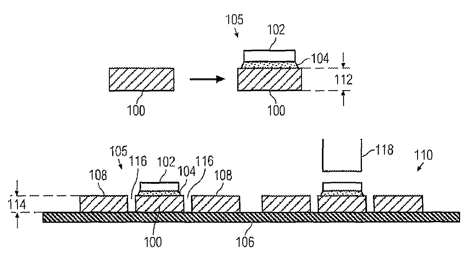
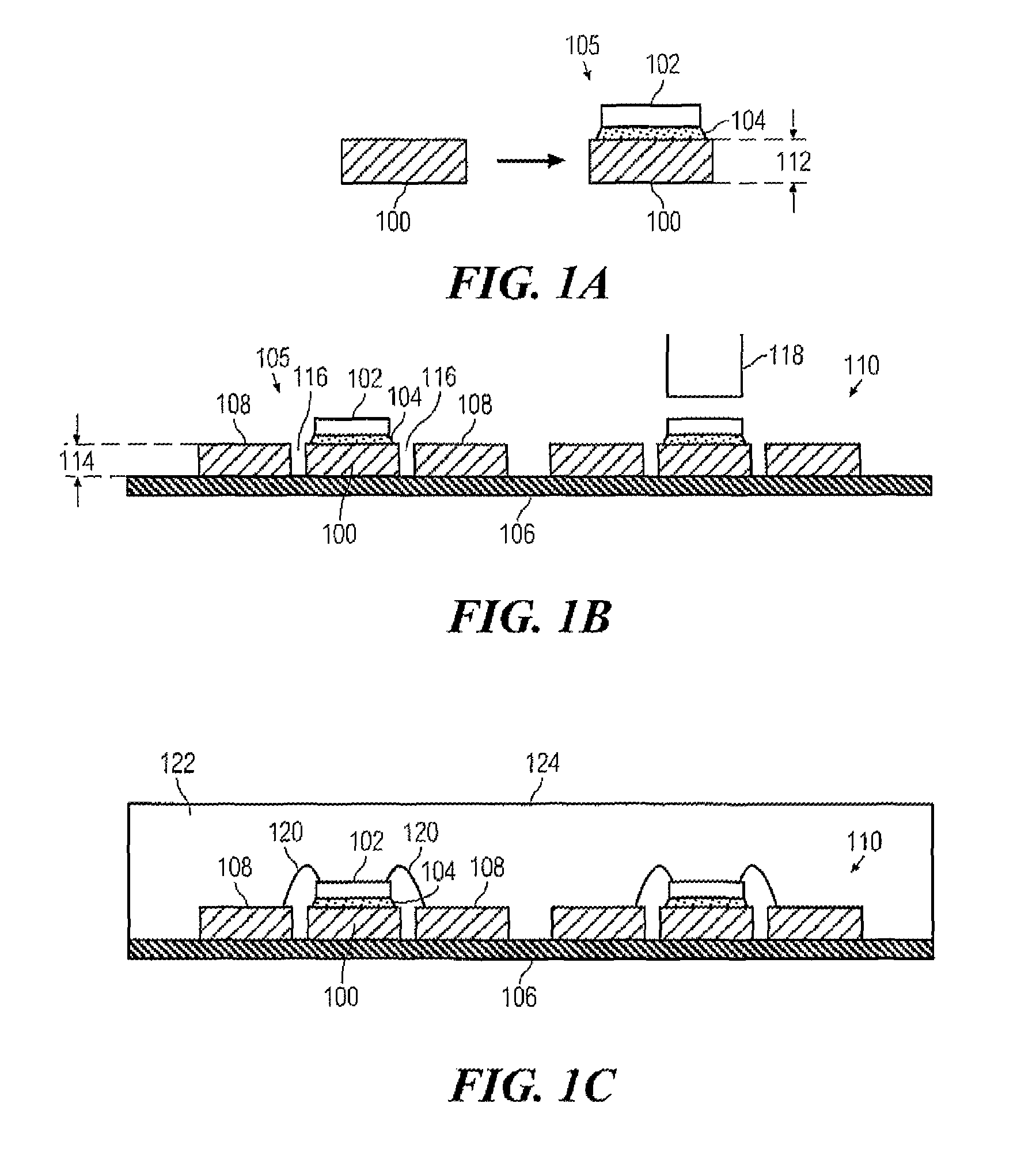
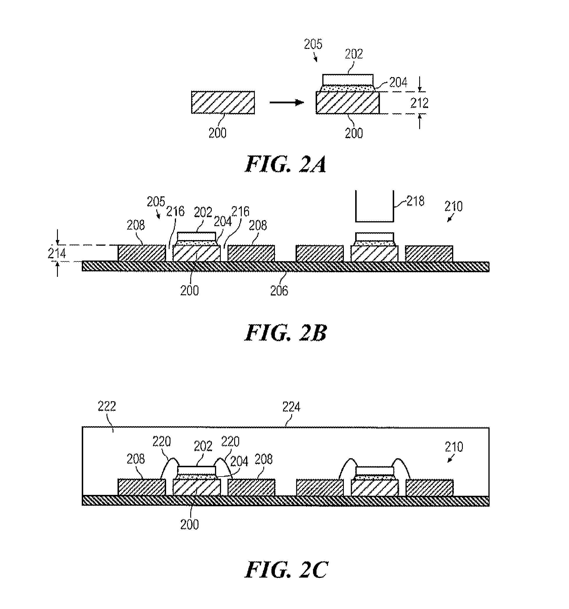
[0026]In one embodiment, the present invention provides a method of forming a semiconductor device, the method comprising affixing a die to a heat sink to form a die and heat sink assembly; and disposing the die and heat sink assembly on a support element of the semiconductor device.

[0027]In another embodiment, the present invention provides a method of forming a semiconductor device, the method comprising affixing a die to a die pad to form a die and die pad assembly; and disposing the die and die pad assembly on a support element of the semiconductor device.

[0028]In yet another embodiment, the present invention provides a semiconductor device comprising a die and heat sink assembly disposed on a support element of the semiconductor device, the die and heat sink having been pre-assembled prior to being disposed on the support element.

[0029]Implementation of embodiments of the invention may provide significant technical benefits in comparison to conventional techniques. For instance...


PUM


Abstract

A method of forming a semiconductor device includes affixing a die to a heat sink to form a die and heat sink assembly and then placing the die and heat sink assembly on a support element. A semiconductor device includes a die and heat sink assembly disposed on a support element. The die and heat sink assembly is pre-assembled prior to being disposed on the support element.

Description

BACKGROUND OF THE INVENTION[0001]The present invention relates to semiconductor devices and methods of assembling semiconductor devices and, more particularly, to methods for improving heat dissipation of semiconductor devices.[0002]Conventional techniques for forming semiconductor devices for high current and / or high-power applications typically involve mounting the power die onto a die pad, which functions as a heat sink to improve dissipation of heat generated by the power die. A die pad, typically formed of metallic material, of a relatively high thickness is required.[0003]Currently, there are two principal techniques to achieve this increased-thickness heat sink, either using a lead frame of increased thickness or using a dual-gauge lead frame. Implementing either technique makes the lead frame significantly more expensive than would otherwise be necessary, thereby making the overall cost of the packaging process undesirably high. The increased thickness also introduces its ow...

Claims


Application Information

Patent Timeline
Patent Type & Authority Patents(United States)
IPC IPC(8): H01L29/66
CPCH01L2224/32225H01L23/49513H01L23/13H01L2224/48257H01L2224/48227H01L2924/15311H01L2224/73265H01L25/0655H01L2224/32245H01L2224/97H01L2924/01029H01L2224/291H01L2224/92247H01L23/3128H01L23/49575H01L24/97H01L23/49816H01L23/3107H01L23/4334H01L21/568H01L23/49568H01L24/32H01L24/48H01L2924/19105H01L2224/2919H01L24/29H01L2224/48247H01L2924/181H01L24/73H01L2224/49109H01L2924/00014H01L24/49H01L2924/00012H01L2924/00011H01L2924/014H01L2224/83H01L2224/85H01L2924/00H01L2224/32145H01L2224/45099H01L2224/45015H01L2924/207
Inventor GAO, WEIGONG, ZHIWEIYE, DEHONGZHANG, HUCHANG
Owner NXP USA INC
Learn More