Stable cold field emission electron source

a cold field emission and electron source technology, applied in the field of cold field emission electron sources, can solve the problems of cfe sources that have shown a tendency for very fast (0.5 to 1.5 hours) quenching of emission current, still demonstrate noise in emission current, etc., and achieve the effect of improving emission stability and reducing nois

Active Publication Date: 2014-05-27
FEI CO
View PDF22 Cites 22 Cited by
  • Summary
  • Abstract
  • Description
  • Claims
  • Application Information

AI Technical Summary

Benefits of technology

[0003]An object of the invention is to provide a cold field emitter (CFE) electron source having improved emission stability and reduced noise.
[0004]In some embodiments of the invention, a filament positioned between an emitter enclosure electrode and an extractor electrode is used to clean surfaces near the emitter tip. In some embodiments, the gap between the emitter enclosure electrode and the extractor electrode is configured to limit the paths of backscattered electrons and / or to reduce the influx of gas molecules into the region of the tip. Embodiments of the invention have been shown to significantly improve stability and reduce the noise of CFEs.

Problems solved by technology

Unfortunately, CFE sources have also shown a tendency for very fast (˜0.5 to 1.5 hours) quenching of the emission current even in excellent UHV (˜10−10 Torr) conditions.
These improved CFE sources, however, still demonstrate noise in the emission current after a short period of source operation.

Method used


Image

  • Stable cold field emission electron source
  • Stable cold field emission electron source
  • Stable cold field emission electron source

Examples


first embodiment

of the Emitter Tip Region

[0038]FIG. 7 is a schematic diagram of a portion of a cold field emitter electron source, illustrating a first embodiment 700 of the emitter tip region. The emitter wire 702 has a sharpened end 703 which emits electrons 710 under the influence of a high electric field induced at tip 703 by a high voltage applied between the emitter tip 703 and extractor 708. A volume enclosing tip 703 is formed between the inner surfaces of emitter enclosure electrode (EEE) 752 and extractor 708. A cleaning filament 730 is shown between the EEE 752 and the extractor 708. An important consideration in the design of the source region for this first embodiment is the aspect ratio between the outer radii of EEE 752 and extractor 708, and the gap separating the inner surfaces of EEE 752 and extractor 708. The larger this aspect ratio, the more backscattered electrons generated from the inner surface of extractor 708 are prevented from striking other (possibly unclean) surfaces wi...

second embodiment

of the Emitter Tip Region

[0039]FIG. 8 is a schematic diagram of a portion of a cold field emitter electron source of the present invention, illustrating a second embodiment 800 of the emitter tip region. The emitter wire 802 has a sharpened end 803 which emits electrons 810 under the influence of a high electric field induced at tip 803 by a high voltage applied between the emitter tip 803 and extractor 808. A cleaning filament 830 is shown between the EEE 852 and the extractor 808. A volume enclosing tip 803 is formed between the inner surfaces of emitter enclosure electrode (EEE) 852 and extractor 808. For this embodiment, extractor 808 has an outer shield ring 890, which prevents the escape of backscattered electrons 871 emitted from area 804 on extractor 808, and backscattered electrons 872 reflected off EEE 852, as shown. The benefits of improved BSE containment in this second embodiment must be balanced against a slightly reduced pumping speed from the source tip region. An ad...

third embodiment

of the Emitter Tip Region

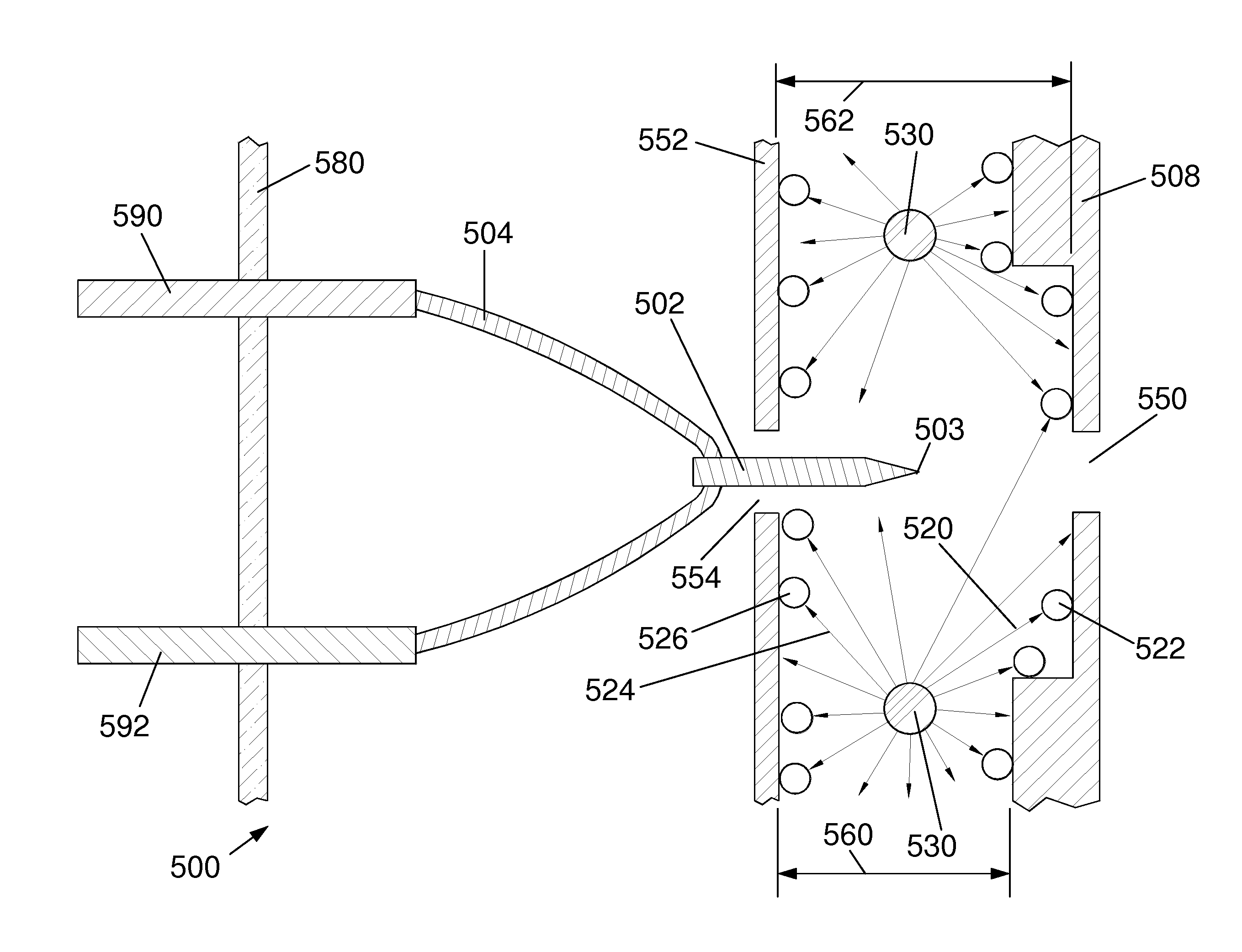
[0040]FIG. 9 is a schematic diagram of a portion of a cold field emitter electron source of the present invention, illustrating a third embodiment 900 of the emitter tip region. The emitter wire 902 has a sharpened end 903 which emits electrons 910 under the influence of a high electric field induced at tip 903 by a high voltage applied between the emitter tip 903 and extractor 908. A cleaning filament 930 is shown between the EEE 952 and the extractor 908. A volume enclosing tip 903 is formed between the inner surfaces of emitter enclosure electrode (EEE) 952 and extractor 908. For this embodiment, EEE 952 has an outer shield ring 990, which prevents the escape of backscattered electrons 971 emitted from area 904 on extractor 908, and backscattered electrons 972 reflected off EEE 952, as shown. The benefits of improved BSE containment in this third embodiment must be balanced against a slightly reduced pumping speed from the source tip region. An additional...


PUM


Abstract

A cold field emission (CFE) electron source for a focused electron beam system such as a transmission electron microscope (TEM), scanning transmission electron microscope (STEM), or scanning electron microscope (SEM) is disclosed. The source employs an emitter enclosure electrode behind the CFE tip which, in conjunction with the extractor electrode, defines a closed volume that can be thoroughly cleaned by electron impact desorption (EID) and radiative heating from a heated filament located between the emitter enclosure electrode and extractor electrode. The extractor electrode may have a counterbore which restricts backscattered electrons generated at the extractor from reaching portions of the source and gun which have not been cleaned by EID. Pre-cleaning of the emitter enclosure electrode and extractor electrode prior to cold field emission substantially improves both source emission stability and frequency noise characteristics, enabling source operation over time intervals adequate for application to TEMs, STEMs, and SEMs.

Description

TECHNICAL FIELD OF THE INVENTION[0001]The present invention relates generally to electron sources, and more particularly to cold field emission electron sources for application in focused electron beam systems.BACKGROUND OF THE INVENTION[0002]In focused electron beam systems a column is typically used to focus an electron beam onto the surface of a target to be imaged and (optionally) processed using the beam. In these columns, an electron source generates the initial beam of electrons, which then passes into an electron “gun”, which typically focuses the charged particles into a roughly parallel beam which enters the main body of the column. Various types of electron sources have been used in focused electron beam systems, including thermionic cathodes, Schottky emitters, and cold field emitters (CFEs). Of these, CFEs are characterized by the highest brightnesses and smallest energy spreads, potentially enabling the smallest beam sizes at the target, with the highest current densit...

Claims


Application Information

Patent Timeline
Patent Type & Authority Patents(United States)
IPC IPC(8): H01J25/50H01J23/06
CPCH01J2237/022H01J37/073H01J23/06H01J37/063
Inventor LIU, KUNSCHWIND, GREGORY A.
Owner FEI CO
Why Eureka
Try Eureka